Alignment method of wafer and mask plate and overlay method of nano structure

A mask plate and wafer technology, applied in the field of overlay technology, can solve the problems of high cost, poor compatibility and inheritance of supporting technologies, offset between exposure patterns and actual positions, etc., achieve high-precision overlay alignment, improve overlay engraving accuracy, to achieve the effect of engraving alignment

Pending Publication Date: 2022-07-12
SHANGHAI CHUANXIN SEMICON CO LTD
View PDF1 Cites 0 Cited by
  • Summary
  • Abstract
  • Description
  • Claims
  • Application Information

AI Technical Summary

Problems solved by technology

However, it cannot be applied to the overlay process of near-working distance gap imaging lithography. At present, the current near-working distance gap imaging lithography is based on the principle of optical microscopy to achieve overlay. However, for the principle of traditional optical microscopy, its resolution There is a 1 / 4 wavelength linewidth resolution limit
The wavelength of the light source used is narrowed from the ultraviolet band (g-line and i-line of mercury lamp) to the 193nm deep ultraviolet band. If you enter into a shorter wavelength light source, such as extreme ultraviolet (EUV), X-ray, etc., not only is it difficult to obtain a high-power light source, but the cost is high , and the supporting technology has poor compatibility and inheritance
Therefore, affected by the resolution limit of traditional optical microscope technology, it is easy to cause the exposure pattern to deviate from the actual position, which affects the overlay accuracy of the lithography machine, and then affects the performance of the semiconductor device.

Method used


Image

  • Alignment method of wafer and mask plate and overlay method of nano structure
  • Alignment method of wafer and mask plate and overlay method of nano structure
  • Alignment method of wafer and mask plate and overlay method of nano structure

Examples


Embodiment Construction

[0031] The technical solutions of the present invention will be clearly and completely described below with reference to the accompanying drawings. Obviously, the described embodiments are a part of the embodiments of the present invention, but not all of the embodiments. Based on the embodiments of the present invention, all other embodiments obtained by those of ordinary skill in the art without creative efforts shall fall within the protection scope of the present invention.

[0032] In addition, the technical features involved in the different embodiments of the present invention described below can be combined with each other as long as they do not conflict with each other.

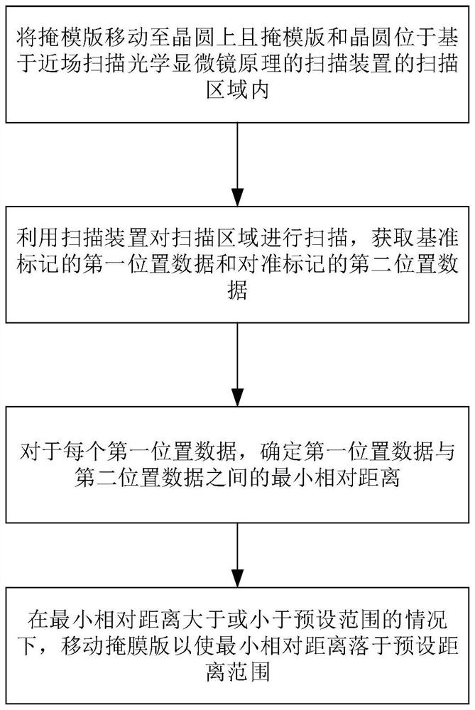
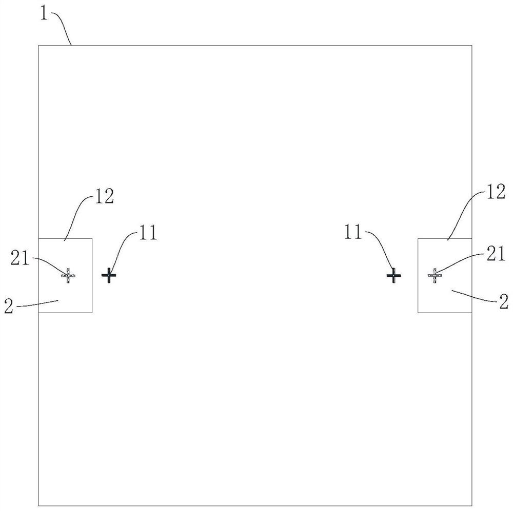
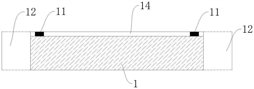
[0033] See figure 1 and combine figure 2 and image 3 , the method for aligning a wafer and a reticle shown in an embodiment of the present invention (Embodiment 1) is applied to the field of near-field lithography to align and position the reticle 1 and the wafer 2 . The reticle 1 includes two a...


PUM


Abstract

The invention relates to a wafer and mask alignment method and a nanostructure overlay method, and the alignment method comprises the steps: S1, moving a mask to a wafer, and enabling the mask and the wafer to be located in a scanning region of an imaging device based on a near-field scanning optical microscope principle, the reference benchmark used for being aligned with the mask plate moved to the wafer in the step is exposed; s2, scanning the scanning area by using a scanning device to obtain first position data of the reference mark and second position data of the alignment mark; s3, for each piece of first position data, determining a minimum relative distance between the first position data and the second position data; and S4, moving the mask plate to enable the minimum relative distance to be within a preset distance range. According to the wafer and mask alignment method and the nanostructure overlay method, optical imaging under the nanoscale can be realized, so that high-precision overlay alignment is realized.

Description

technical field [0001] The invention relates to an alignment method of a wafer and a mask and a nanostructure overlay method, which are applied to overlay technology and belong to the technical field of semiconductors. Background technique [0002] In a manufacturing process of a semiconductor device, when a stacked structure having a circuit pattern of a semiconductor device is formed, a photolithography process is performed on each layer. In the circuit pattern, connections must also be formed between the upper and lower layers. Therefore, the overlay accuracy of the patterns of the respective layers is important. At present, in the field of semiconductors such as microelectronics, the realization of overlay through reticle usually includes three categories: projection method (achieved by projection lithography machine), nanoimprint technology and contact lithography technology (that is, generalized contact lithography technology) The generalized contact lithography tech...

Claims


Application Information

Patent Timeline
Patent Type & Authority Applications(China)
IPC IPC(8): G03F9/00
CPCG03F9/70G03F9/7088
Inventor 林岳明季明华
Owner SHANGHAI CHUANXIN SEMICON CO LTD
Why Eureka
Try Eureka