Eureka AIR delivers breakthrough ideas for toughest innovation challenges, trusted by R&D personnel around the world.

Device and method for measuring thickness of dielectric layer in circuit board

A dielectric layer and circuit board technology, which is applied in the field of measurement devices that use induction components to measure the thickness of the dielectric layer in the circuit board, can solve the problems of time-consuming and labor-intensive, circuit board scrapping, and circuit board damage, and achieve small area effect

Pending Publication Date: 2022-07-19
UNIMICRON TECH CORP
View PDF0 Cites 0 Cited by
  • Summary
  • Abstract
  • Description
  • Claims
  • Application Information

AI Technical Summary

Problems solved by technology

However, this measurement method is very time-consuming and labor-intensive, and also damages a large area of ​​the circuit board, making the circuit board scrapped

Method used


Image

  • Device and method for measuring thickness of dielectric layer in circuit board
  • Device and method for measuring thickness of dielectric layer in circuit board
  • Device and method for measuring thickness of dielectric layer in circuit board

Examples


Embodiment Construction

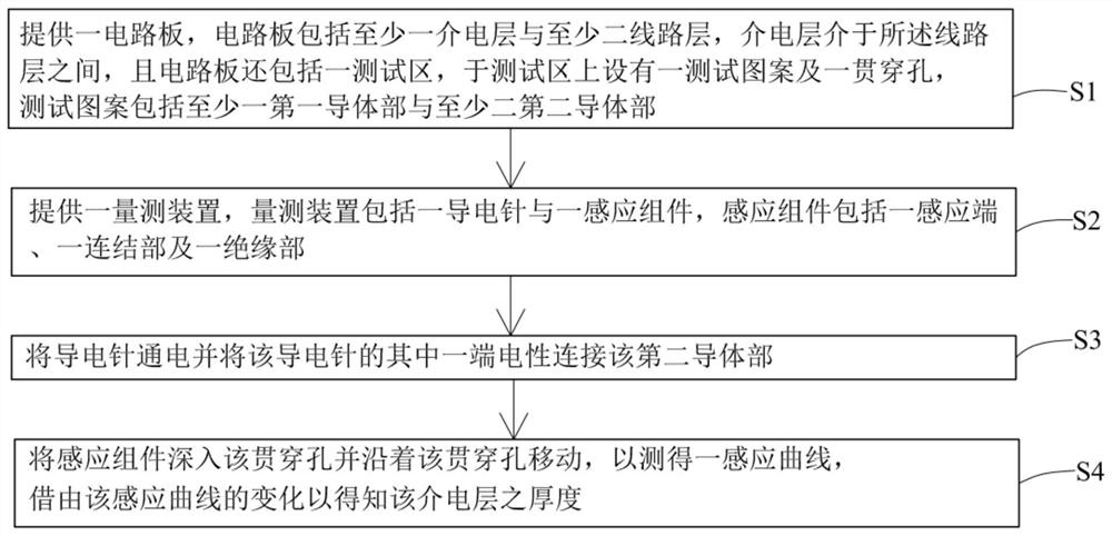
[0026] see figure 1 , figure 1 The drawing is a schematic diagram of the method for measuring the thickness of the dielectric layer in the circuit board of the present invention. The measurement method of the thickness of the dielectric layer in the circuit board includes the following steps:

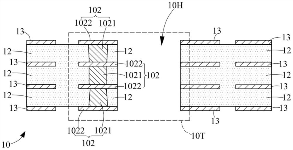
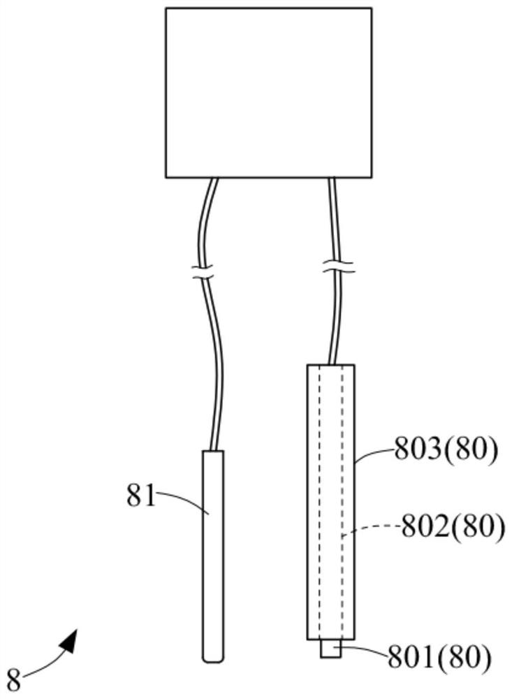
[0027] First, please refer to step S1 and Figure 2A , Figure 2A The drawing is a partial cross-sectional schematic diagram of the circuit board 10, and a circuit board 10 is provided. The circuit board 10 includes three layers of dielectric layers 12 and four layers of circuit layers 13, but those with ordinary knowledge in the art should be able to understand the circuit board 10 in practice. More layers of dielectric layers 12 and circuit layers 13 may be included, or the circuit board 10 may also include only one layer of dielectric layer 12 and two layers of circuit layers 13 . Moreover, the dielectric layer 12 is interposed between the two circuit layers 13 . In addition, th...


PUM


Abstract

The method for measuring the thickness of the dielectric layer in the circuit board comprises the following steps of: firstly, providing the circuit board which comprises at least one dielectric layer and at least two circuit layers, the dielectric layer is arranged between the circuit layers, the circuit board further comprises a test area, a test pattern and a through hole are arranged on the test area, and the test pattern is arranged on the test area; the test pattern includes at least one first conductor portion and at least two second conductor portions. The distance between the side edge of the through hole and the second conductor part is smaller than the distance between the side edge of the through hole and the first conductor part. Afterwards, a measuring device is provided, and the measuring device comprises a conductive needle and a sensing assembly. Then, the conductive needle is electrified, and one end of the conductive needle is electrically connected with the second conductor part. Afterwards, the sensing component goes deep into the through hole and moves along the through hole so as to measure a sensing curve, and the thickness of the dielectric layer can be known through the change of the sensing curve. The method has the advantages that the thickness of the dielectric layer of the circuit board can be rapidly and conveniently measured, and the circuit board does not need to be damaged.

Description

technical field [0001] The present invention relates to a measuring device and method for measuring the thickness of a dielectric layer in a circuit board, in particular to a measuring device and a measuring method for measuring the thickness of the dielectric layer in a circuit board using an induction component. Background technique [0002] At present, the thickness of the dielectric layer of the circuit board is mainly measured by destructive methods. For example, a part of the circuit board to be tested must be cut off first, and a measurement slice is made, and then an optical microscope (Optical Microscope) or scanning method is used. Electron microscope (Scanning Electron Microscope) measures the thickness of the dielectric layer of the circuit board. However, this measurement method is very time-consuming and labor-intensive, and also damages a large area of ​​the circuit board and makes the circuit board scrapped. [0003] Therefore, how to quickly and convenientl...

Claims


Application Information

Patent Timeline
Patent Type & Authority Applications(China)
IPC IPC(8): G01B7/06
CPCG01B7/06G01B7/08
Inventor 张成瑞张宏麟
Owner UNIMICRON TECH CORP
Why Eureka
Eureka Blog
Learn More