Method for adjusting uniformity of epitaxial growth

An epitaxial growth, uniform technology, applied in the direction of electrical components, circuits, semiconductor/solid-state device manufacturing, etc., can solve the problems of poor film thickness uniformity, excessive wafer growth, wafer defects, etc., to achieve improved flatness and good growth Uniformity, the effect of avoiding dislocation

Pending Publication Date: 2022-07-22
SHANGHAI HUAHONG GRACE SEMICON MFG CORP
View PDF0 Cites 0 Cited by
  • Summary
  • Abstract
  • Description
  • Claims
  • Application Information

AI Technical Summary

Problems solved by technology

[0003] The in-plane distribution of EPI THK is also a very important part of the EPI process. The uniformity of the film thickness is poor, which may easily lead to local growth of the wafer (wafer) too fast or too slow, resulting in local wafer defects (fail) and dislocation (dislocation) ) or other questions

Method used


Image

  • Method for adjusting uniformity of epitaxial growth

Examples


Embodiment Construction

[0017] The technical solutions in the embodiments of the present invention will be clearly and completely described below with reference to the accompanying drawings in the embodiments of the present invention. Obviously, the described embodiments are only a part of the embodiments of the present invention, rather than all the embodiments.

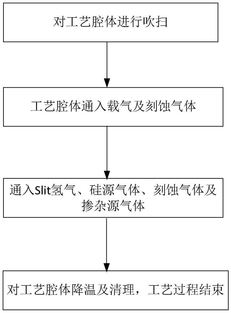
[0018] like figure 1 As shown, the method for adjusting the uniformity of epitaxial growth of the present invention comprises the following steps:

[0019] Step 1: Purging the process chamber (Chamber) to remove the residual process gas, and at the same time, the process chamber starts to heat up.

[0020] In step 2, a carrier gas and an etching gas are introduced into the process chamber, and a high temperature is used to remove the natural oxide layer of the silicon wafer, and the surface of the silicon wafer is smoothed.

[0021] Step 3: After the temperature is lowered to a typical process temperature, Slit hydrogen gas, silicon sourc...


PUM


Abstract

The invention discloses a method for adjusting epitaxial growth uniformity, which comprises the following steps of: 1, purging a process cavity to remove previous process gas residues, and heating the process cavity at the same time; step 2, introducing a carrier gas and an etching gas into the process cavity, removing a natural oxide layer of the silicon wafer by utilizing high temperature, and carrying out smoothing treatment on the surface of the silicon wafer; step 3, after the temperature is reduced to a typical process temperature, introducing Slit hydrogen, silicon source gas, etching gas and doping source gas; and step 4, the EPI growth is finished, the process cavity is cooled and cleaned, and the process is finished. The method has better growth uniformity, and can reduce or eliminate the problem of local over-grinding or residue after chemical mechanical grinding.

Description

technical field [0001] The present invention relates to the field of semiconductors, and in particular, to a method for adjusting the uniformity of epitaxial (EPI) growth. Background technique [0002] In the EPI process, the film thickness (THK) and the in-plane profile (profile) of the film thickness are the key parameters of the entire process. The growth rate of EPI is mainly determined by the flow rate of the silicon source and the reaction temperature. Generally, the higher the temperature, the greater the flow rate of the silicon source, the faster the growth rate, and the higher the film thickness. [0003] The in-plane distribution of EPI THK is also a very important part of the EPI process. The film thickness uniformity is poor, which can easily lead to the local growth of the wafer (wafer) is too fast or too slow, resulting in local wafer defects (fail), resulting in dislocation (dislocation) ) or other problems. SUMMARY OF THE INVENTION [0004] In view of t...

Claims


Application Information

Patent Timeline
Patent Type & Authority Applications(China)
IPC IPC(8): H01L21/205
CPCH01L21/02381H01L21/02532H01L21/02661H01L21/0262H01L21/02634
Inventor 李伟叶侯翔宇李昊
Owner SHANGHAI HUAHONG GRACE SEMICON MFG CORP
Why Eureka
Try Eureka