Method for testing security performance of SRAM (Static Random Access Memory) chip

A technology of safety performance and testing method, applied in the field of testing, can solve the problems of inability to accurately measure the degree of aging, single evaluation variable, etc., to ensure the reliability of data, simplify the calculation process, and save computing resources.

Pending Publication Date: 2022-07-26
INST OF MICROELECTRONICS CHINESE ACAD OF SCI
View PDF0 Cites 0 Cited by
  • Summary
  • Abstract
  • Description
  • Claims
  • Application Information

AI Technical Summary

Problems solved by technology

[0004] In view of the above analysis, the embodiment of the present invention aims to provide a method for testing the safety performance of an S

Method used


Image

  • Method for testing security performance of SRAM (Static Random Access Memory) chip
  • Method for testing security performance of SRAM (Static Random Access Memory) chip
  • Method for testing security performance of SRAM (Static Random Access Memory) chip

Examples


Embodiment 1

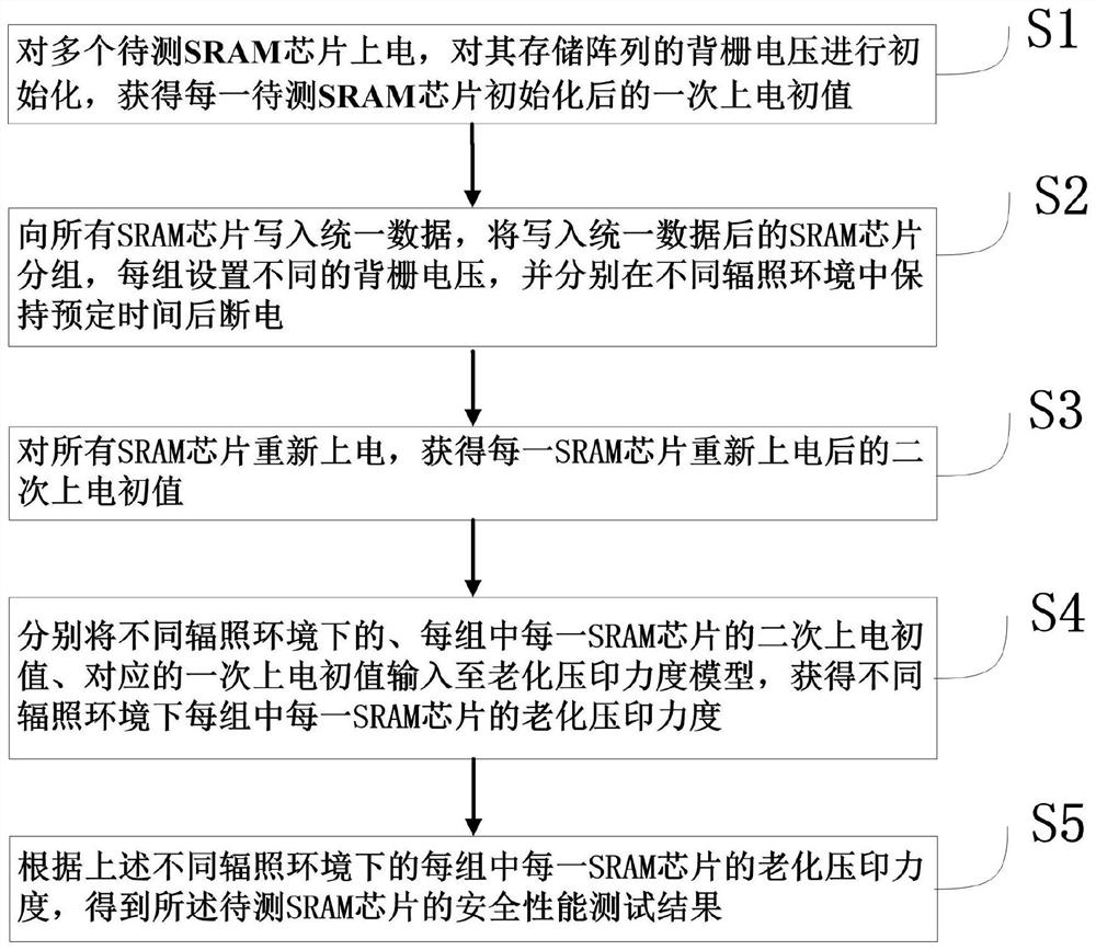
[0058] A specific embodiment of the present invention discloses a method for testing the safety performance of an SRAM chip, such as figure 1 shown, including the following steps:

[0059] S1. Power on multiple SRAM chips to be tested, initialize the back gate voltage of their storage arrays, and obtain an initial power-on value after initialization of each SRAM chip to be tested through statistics;

[0060] S2. Write unified data to all SRAM chips, group the SRAM chips after writing the unified data, set different back gate voltages for each group, and keep the power off after a predetermined period of time in different irradiation environments;

[0061] S3. Re-power on all SRAM chips, and obtain the initial value of the second power-on after re-powering each SRAM chip through statistics;

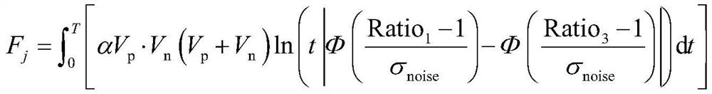
[0062] S4. Respectively input the secondary power-on initial value and the corresponding primary power-on initial value of each SRAM chip in each group under different irradiation environ...

Embodiment 2

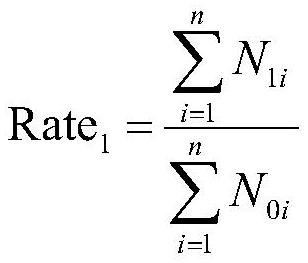
[0067] On the basis of Embodiment 1, optimization is performed, and the initial value of power-on is represented by the ratio of the number of memory cells with a value of 1 to the number of memory cells with a value of 0 in the SRAM chip after power-on.

[0068] Step S1 further includes:

[0069] S11. Connect each SRAM chip to be tested to the test system, and power on the SRAM chip through the test system;

[0070] S12. Set the back gate voltage V of all NMOS transistors and PMOS transistors in the memory array of the SRAM chip BN with V BP All are set to 0V, the initialization is completed, and the number and proportion of 1 and 0 in the storage array after initialization are counted;

[0071] S13. Repeat the process of the above steps S11 to S12 to complete n tests, and sequentially obtain the number and ratio of 1 and 0 in the storage array after the SRAM chip is initialized in the n test results, and for all the number N of 1 and 0 1i , N 0i Calculate the average wit...

Embodiment 3

[0094] The present invention also provides an evaluation system for the safety performance of the SRAM chip corresponding to Embodiment 1 or 2, including a test board, an FPGA chip and a host computer connected in sequence. Wireless communication is possible between the FPGA chip and the host computer.

[0095] The test board is used to access the SRAM chip to be tested, and to adjust the back gate voltages of all NMOS transistors and PMOS transistors in its storage array according to the control of the FPGA chip; and, to output the information stored in the storage array of the SRAM chip to be tested to FPGA chip.

[0096] Through the above test board, each port of the SRAM chip to be tested is led out.

[0097]The FPGA chip is used to send an initialization instruction to the test board during testing, and the initialization instruction is used to set the back gate voltages of all NMOS transistors and PMOS transistors in the storage array of the SRAM chip to be tested to 0V...


PUM


Abstract

The invention relates to a method for testing the safety performance of an SRAM (Static Random Access Memory) chip, belongs to the technical field of chip detection, and solves the problems that the evaluation variable in the prior art is too single and aged imprint cannot be accurately measured. The method comprises the following steps: electrifying a plurality of SRAM chips to be tested, and initializing back gate voltages of storage arrays of the SRAM chips to obtain a primary electrifying initial value of each SRAM chip; writing unified data into all the SRAM chips, grouping the SRAM chips into which the unified data is written, setting different back gate voltages for each group, and respectively keeping the SRAM chips in different irradiation environments for preset time; re-electrifying all the SRAM chips to obtain a secondary electrifying initial value of each SRAM chip; and respectively inputting the secondary power-on initial value of each SRAM chip in different groups and the corresponding primary power-on initial value in different irradiation environments into an aging imprint strength model to obtain the aging imprint strength of each SRAM chip in different irradiation environments, thereby obtaining a safety performance test result of the to-be-tested SRAM chip.

Description

technical field [0001] The invention relates to the technical field of testing, in particular to a method for testing the safety performance of an SRAM chip. Background technique [0002] Before the SRAM chip is put into use, it needs to be tested for its safety performance. In order to protect data security, once the existing security chip system detects unauthorized illegal access, it will cut off the power of the SRAM chip to prevent attackers from stealing data. However, the SRAM chip has the problem of residual information, and will partially restore the information stored before the power failure. That is, when a certain memory cell is used to store fixed data for a long time, the two symmetrical MOS tubes will have different degrees of BTI aging effect, resulting in permanent threshold voltage mismatch, resulting in a certain probability (about 10% to 20%) after the cell is powered on. %) read out the initial power-on value opposite to the original stored value. ...

Claims


Application Information

Patent Timeline
IPC IPC(8): G11C29/56
CPCG11C29/56
Inventor 李博苏泽鑫宿晓慧王磊卜建辉赵发展韩郑生
Owner INST OF MICROELECTRONICS CHINESE ACAD OF SCI
Why Eureka
Try Eureka