Wide bandgap semiconductor ultraviolet detector imaging system and method based on galvanometer scanning
A wide-bandgap semiconductor and ultraviolet detector technology, used in instruments, image enhancement, image data processing, etc., can solve the problems of low image signal-to-noise ratio and low detection accuracy, restore clear images and reduce overlapping. Effect
- Summary
- Abstract
- Description
- Claims
- Application Information
AI Technical Summary
Problems solved by technology
Method used
Image
Examples
Embodiment 1
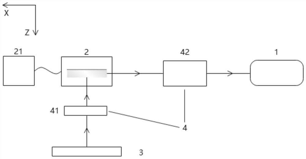
[0056] This embodiment provides an imaging system based on a wide-bandgap semiconductor ultraviolet detector, such as figure 1 As shown, it includes a wide bandgap semiconductor ultraviolet detector 1, a two-dimensional galvanometer module 2, a triggering device 21, a target area 3 and a scanning pixel limiting module 4, wherein:
[0057] The target area 3 emits solar-blind ultraviolet rays, which are received by the wide-bandgap semiconductor ultraviolet detector 1 after passing through the two-dimensional galvanometer module 2;
[0058] The triggering device 21 is connected with the two-dimensional galvanometer module 2, and the triggering device 21 controls the working state of the two-dimensional galvanometer module 2, so that at a certain moment, only one determination is made in the target area 3. The light emitted from the small area of is only received by the wide-bandgap semiconductor ultraviolet detector 1 after passing through the two-dimensional galvanometer mo...
Embodiment 2
[0062] On the basis of Embodiment 1, this embodiment continues to disclose the following content:
[0063] The response band of the material used in the wide-bandgap semiconductor ultraviolet detector 1 is in the solar blind region, and an AlGaN-based solar blind ultraviolet detector is used in this embodiment.
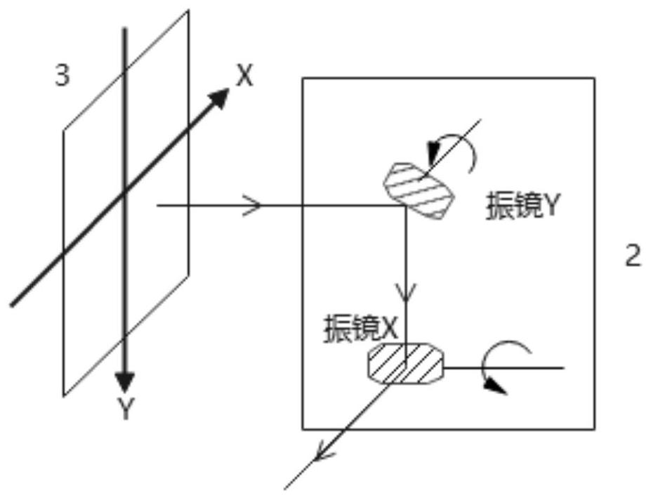
[0064] like figure 2 As shown in the figure, the two-dimensional galvanometer module 2 includes a galvanometer X and a galvanometer Y whose scanning directions are orthogonal, and reflects light beams in different small areas within the field of view at different times through vibration. At a certain moment, the target area 3 The light emitted by a certain small area in the interior is successively received by the wide-bandgap semiconductor ultraviolet detector 1 through the reflection of the galvanometer Y and the galvanometer X, and the trigger device 21 inputs an electrical signal to the two-dimensional galvanometer module 2 to drive The galvanometer X and the ga...
Embodiment 3
[0069] This embodiment provides a wide-bandgap semiconductor ultraviolet detector imaging method based on galvanometer scanning, such as Figure 4 As shown, the method is applied to the wide-bandgap semiconductor ultraviolet detector imaging system based on galvanometer scanning according to any one of claims 1 to 5, and the method includes the following steps:
[0070] S1: the triggering device 21 inputs a control signal to drive the two-dimensional galvanometer module 2 to scan;
[0071] S2: the solar-blind ultraviolet light signal of the target area 3 is acquired by the wide-bandgap semiconductor ultraviolet detector 1 through the two-dimensional galvanometer module 2 and the scanning pixel limiting module 4;
[0072] S3: The image waveform of the target area 3 is obtained by photoelectric conversion from the wide-bandgap semiconductor ultraviolet detector 1, and is restored to the original image;
[0073] S4: Deconvolution operation is performed on the original image to o...
PUM
 Abstract
Description
Claims
Application Information


