Application of planar carrier plate in wafer bearing
A wafer carrying and wafer technology, which is applied in the manufacture of electrical components, circuits, semiconductors/solid-state devices, etc., can solve problems such as the inability to meet the high temperature process of wafers, the poor high temperature resistance of adhesives, and the inability to stabilize wafers. , to achieve the effect of overcoming the temperature limit, simple production, and low material cost
- Summary
- Abstract
- Description
- Claims
- Application Information
AI Technical Summary
Problems solved by technology
Method used
Image

Examples
Embodiment 1
[0028] An application of a plane carrier plate in wafer carrying, characterized in that, the surface of the plane carrier plate is provided with a number of air suction holes for adsorbing wafers, and the application method specifically includes the following steps:
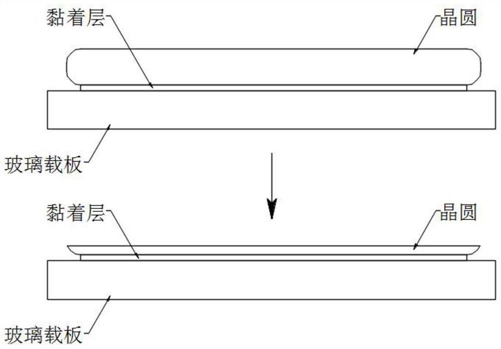
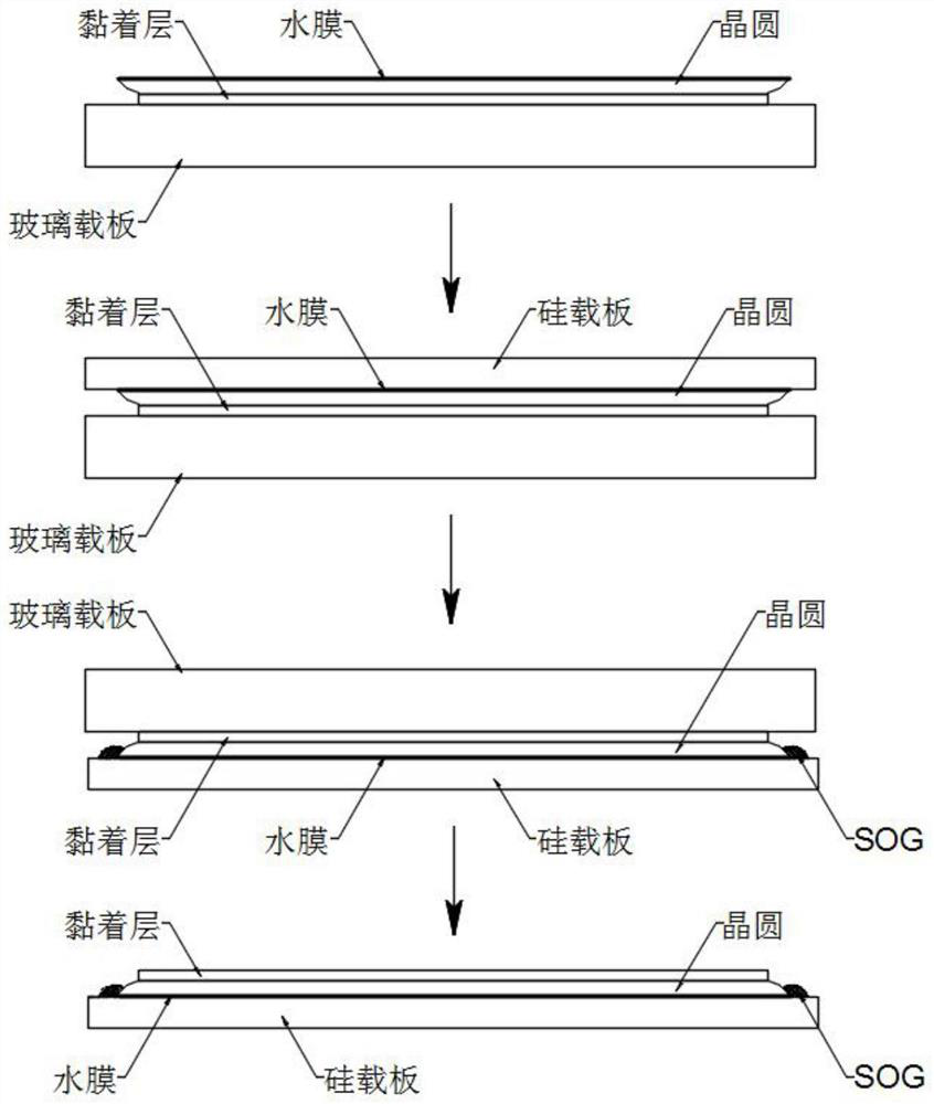
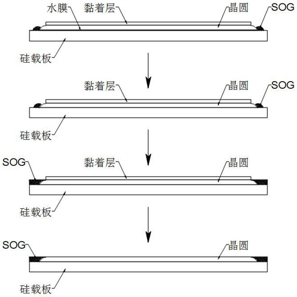
[0029] S1. On the front side of the wafer where the ILD process and the contact hole opening are completed, the glass carrier is bonded with an adhesive, and then the back side of the wafer is thinned by grinding / etching, and the ion implantation process on the back side of the wafer is completed;
[0030] S2. Spray deionized water on the back of the wafer to form a water film with a uniform thickness, and then attach a silicon carrier to the back of the wafer. With the help of the gravitational force between water molecules and the external atmospheric pressure, the silicon carrier is connected to the wafer. Adsorb, then turn the glass carrier plate, the wafer and the silicon carrier plate as a whole, apply SOG t...
Embodiment 2
[0035] An application of a plane carrier plate in wafer carrying, characterized in that, the surface of the plane carrier plate is provided with a number of air suction holes for adsorbing wafers, and the application method specifically includes the following steps:
[0036] S1. On the front side of the wafer where the ILD process and the contact hole opening are completed, the glass carrier is bonded with an adhesive, and then the back side of the wafer is thinned by grinding / etching, and the particle implantation process on the back side of the wafer is completed;
[0037] S2. Spray deionized water on the back of the wafer to form a water film with a uniform thickness, and then attach a silicon carrier to the back of the wafer. With the help of the gravitational force between water molecules and the external atmospheric pressure, the silicon carrier is connected to the wafer. Adsorb, then turn the glass carrier plate, the wafer and the silicon carrier plate as a whole, apply ...
PUM
 Abstract
Description
Claims
Application Information
PatSnap Eureka turns technology decisions into work you can execute. Powered by our Innovation Knowledge Graph, it runs expert workflows across engineering, life sciences, materials and intellectual property. Get your review-ready output in minutes.


