High-flatness printed circuit board (PCB) embedded with ceramic blocks and preparation process of high-flatness PCB

A technology of PCB board and preparation process, which is applied in the manufacture of printed circuits, printed circuits connected with non-printed electrical components, printed circuit components, etc. The effect of low cost and simple preparation process

Pending Publication Date: 2022-07-29
CHENGYI ELECTRONICS JIAXING
View PDF6 Cites 0 Cited by
  • Summary
  • Abstract
  • Description
  • Claims
  • Application Information

AI Technical Summary

Problems solved by technology

The thickness of the conventional release film is 50um, and the release film below 50um is not suitable for mass production of PCB boards due to the high production difficulty, while the release film with a thickness of 50um can reach ±30um during the lamination process. Therefore, such conventional methods cannot meet the high flatness requirement of ±5um for COB packaging products

Method used


Image

  • High-flatness printed circuit board (PCB) embedded with ceramic blocks and preparation process of high-flatness PCB
  • High-flatness printed circuit board (PCB) embedded with ceramic blocks and preparation process of high-flatness PCB

Examples


Embodiment Construction

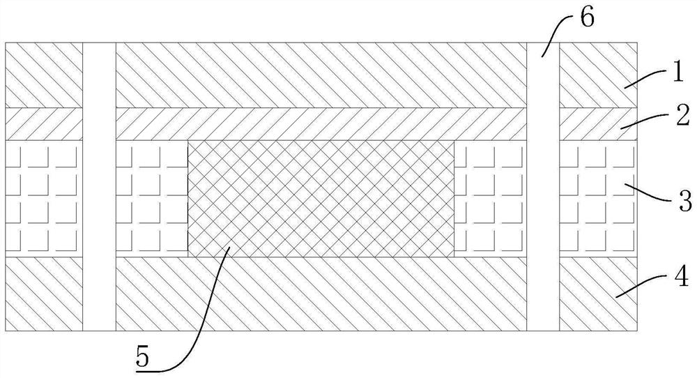
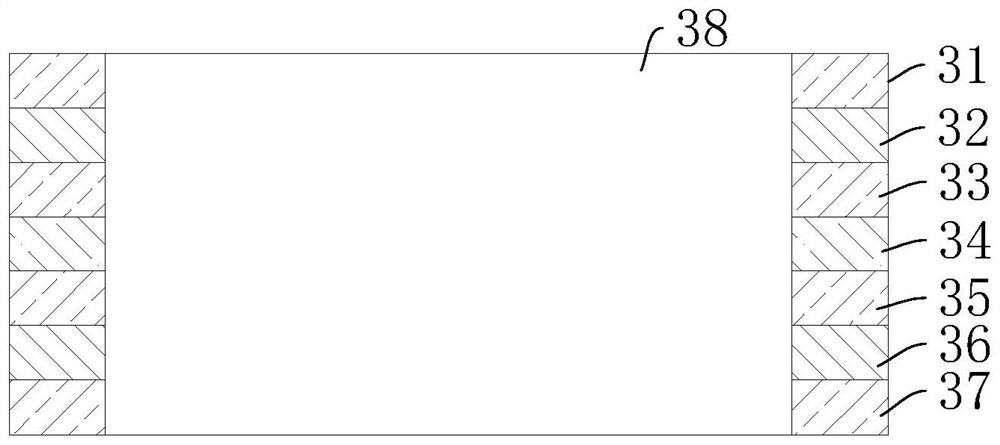
[0031] In order to make those skilled in the art better understand the technical solutions of the present invention, the preferred embodiments of the present invention will be described below in conjunction with specific embodiments, but it should be understood that the accompanying drawings are only used for exemplary illustration, and should not be construed as a reference to the present invention. Limitation; in order to better illustrate this embodiment, some parts of the drawings will be omitted, enlarged or reduced, which do not represent the size of the actual product; for those skilled in the art, some well-known structures and their descriptions in the drawings may be The omission is understandable. The positional relationships described in the drawings are only for exemplary illustration, and should not be construed as a limitation on the present patent.

[0032] In the present invention, the release steel plate is formed by coating a release liquid with a thickness ...


PUM

PropertyMeasurementUnit
sizeaaaaaaaaaa

Abstract

The invention discloses a high-flatness printed circuit board (PCB) embedded with ceramic blocks and a preparation process thereof, the high-flatness PCB embedded with ceramic blocks comprises a PCB body, the PCB body comprises a conventional steel plate, a release film, a PCB layer and a release steel plate which are laminated from top to bottom; the PCB layer comprises a first circuit layer, a first core layer, a second circuit layer, a PP bonding layer, a third circuit layer, a second core layer and a fourth circuit layer which are formed by hot melting from top to bottom; the middle part of the PCB layer is provided with an empty groove used for installing a ceramic block. And the empty slot penetrates through the first circuit layer, the first core layer, the second circuit layer, the PP bonding layer, the third circuit layer, the second core layer and the fourth circuit layer. When the PCB body is pressed, the ceramic block is in direct contact with the release steel plate, so that the high flatness precision of the ceramic block and the surface of the PCB layer is within +/-5 microns, and meanwhile, the preparation process is simple, the manufacturing cost is relatively low, and the PCB is suitable for large-scale production.

Description

technical field [0001] The invention relates to the technical field of PCB boards, in particular to a high flatness embedded ceramic block PCB board and a preparation process thereof. Background technique [0002] With the gradual development of electronic products in the direction of higher signal transmission frequency, smaller size and higher power, embedding ceramic blocks in the carrier PCB board of electronic components has become the first choice for high heat dissipation to meet the increasing demand. Ceramic blocks have better insulation than metal blocks, but at the same time, they have the problem of greater hardness, and it is not easy to grind to the same flatness as the PCB surface after being embedded in the PCB board. The conventional production method is to isolate a layer of release film between the ceramic block and the steel plate in the PCB board during lamination, so as to avoid the resin overflowing around the ceramic block from adhering to the steel p...

Claims


Application Information

Patent Timeline
Patent Type & Authority Applications(China)
IPC IPC(8): H05K1/18H05K1/02H05K3/00
CPCH05K1/185H05K1/0201H05K3/0044H05K3/0061H05K3/0047
Inventor 张本贤李志雄舒志迁魏和平陈蓁邱锡曼
Owner CHENGYI ELECTRONICS JIAXING
Why Eureka
Try Eureka