Ultraviolet device packaging structure and manufacturing method

A device packaging and ultraviolet technology, applied in semiconductor devices, electrical components, circuits, etc., can solve the problems of inability to output deep ultraviolet radiation energy, performance degradation, and reduction of sterilization and disinfection effects, to improve the sterilization and disinfection effect, increase radiation energy, The effect of enhancing the sterilization and disinfection effect

Inactive Publication Date: 2022-08-05
ZHIXIN SEMICON (HANGZHOU) CO LTD
View PDF8 Cites 1 Cited by
  • Summary
  • Abstract
  • Description
  • Claims
  • Application Information

AI Technical Summary

Problems solved by technology

The deep ultraviolet light-emitting diode chip package in the prior art is affected by the atmosphere, resulting in performance degradation, unable to output higher deep ultraviolet radiation energy, and reducing the sterilization effect

Method used


Image

  • Ultraviolet device packaging structure and manufacturing method
  • Ultraviolet device packaging structure and manufacturing method
  • Ultraviolet device packaging structure and manufacturing method

Examples


Embodiment Construction

[0032] The technical solutions in the embodiments of the present invention will be clearly and completely described below with reference to the accompanying drawings in the embodiments of the present invention. Obviously, the described embodiments are only a part of the embodiments of the present invention, rather than all the embodiments. Based on the embodiments of the present invention, all other embodiments obtained by those of ordinary skill in the art without creative efforts shall fall within the protection scope of the present invention.

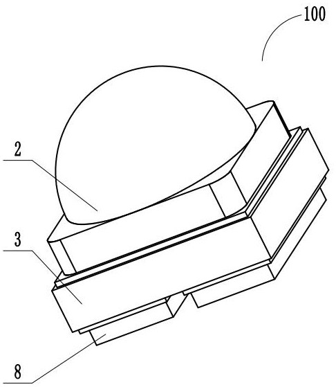
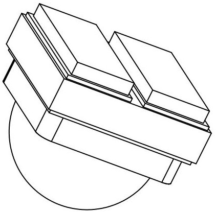
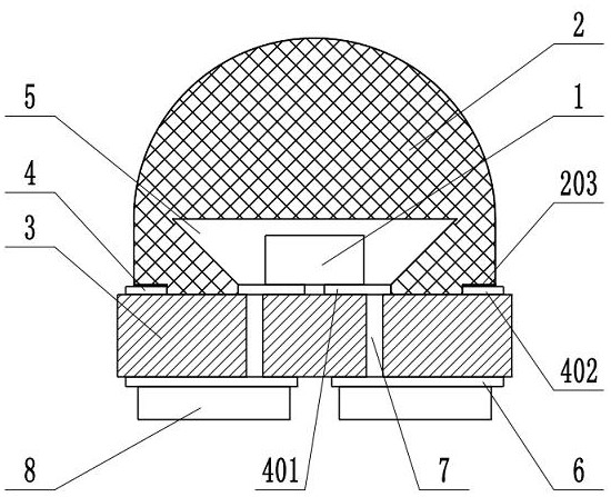
[0033] The purpose of the present invention is to provide an ultraviolet device packaging structure and a manufacturing method, so as to solve the above-mentioned problems in the prior art, avoid the chip being affected by the atmosphere, and improve the radiation energy of the deep ultraviolet light emitting diode.

[0034] In order to make the above objects, features and advantages of the present invention more clearly understood, t...


PUM

PropertyMeasurementUnit
wavelengthaaaaaaaaaa

Abstract

An ultraviolet device packaging structure disclosed by the present invention comprises a chip, a lens and a substrate, the chip is arranged in a light-condensing accommodating hole of the lens, the chip can be conducted with an external element by using a first conduction element, the substrate blocks the accommodating hole, the chip is packaged in a packaging cavity, and the packaging cavity is filled with a protective gas. Inert gases such as nitrogen can be selected as the protective gas, and the chip is prevented from being influenced by the atmosphere, so that the radiation energy of the deep ultraviolet light-emitting diode is improved, and the sterilization and disinfection effects of the deep ultraviolet light-emitting diode are enhanced. Meanwhile, the invention further provides a manufacturing method of the ultraviolet device packaging structure, a eutectic furnace is used for enabling protective gas to enter the space between the substrate and the lens, eutectic welding is achieved between the first conduction element and the lens, the chip and the protective gas are packaged in the packaging cavity, and therefore the influence of the atmosphere on the chip is effectively avoided, and the packaging quality of the ultraviolet device is improved. And the performance of the deep ultraviolet light-emitting diode is improved.

Description

technical field [0001] The present invention relates to the technical field of semiconductor packaging, in particular to an ultraviolet device packaging structure and a manufacturing method. Background technique [0002] Deep ultraviolet light emitting diode (UVC LED) is a high power deep ultraviolet light emitting diode with a wavelength between 220nm and 350nm. The deep ultraviolet light emitting diode has high reliability, long life, fast response, low power consumption, environmental protection, no pollution, small size, etc. Advantages, it is widely used in the fields of sterilization, water purification, medical treatment, high-density optical recording, high color rendering LED lighting and high-speed decomposition and treatment of pollution substances. [0003] It is worth noting that due to the material and structure of the deep ultraviolet light emitting diode chip, the current TE light output of the deep ultraviolet light emitting diode chip is weaker than the sid...

Claims


Application Information

Patent Timeline
Patent Type & Authority Applications(China)
IPC IPC(8): H01L33/58H01L33/60H01L33/62H01L33/48
CPCH01L33/58H01L33/60H01L33/62H01L33/486H01L2933/0033H01L2933/0058H01L2933/0066
Inventor 不公告发明人
Owner ZHIXIN SEMICON (HANGZHOU) CO LTD
Why Eureka
Try Eureka