Process for producing semiconductor article
A semiconductor and product technology, applied in the field of semiconductor product manufacturing, can solve problems such as difficult heat treatment, and achieve the effect of easy separation and cost reduction
- Summary
- Abstract
- Description
- Claims
- Application Information
AI Technical Summary
Problems solved by technology
Method used
Image
Examples
Embodiment 1
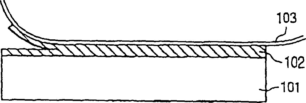
[0113] The process of the semiconductor product in this embodiment includes the steps of forming a porous layer on at least one main surface of the substrate, bonding a film to the surface of the porous layer, and separating the substrate side and the film side at the porous layer. Refer below Figures 1A to 1D Introduce craft.
[0114] Porous Si layer 102 is formed on the main surface of first single crystal Si substrate 101 ( Figure 1A ). On the surface of the porous Si layer, a flexible adhesive film 103 or a flexible film is bonded to the surface of the porous Si layer with an adhesive (FIG. 1B). Of course, in this embodiment and other embodiments described later, the films are adhered with conductive paste. Then, the flexible film was peeled off from the first single crystal Si substrate 101, thereby separating the substrate side and the film side at the porous Si layer ( Figure 1C ). Thus the thin porous Si film is separated from the Si substrate 101 ( Figure 1D ...
Embodiment 2
[0117] The process in this embodiment includes the steps of forming a porous layer on at least one major surface of a first substrate, bonding a film to the surface of the non-porous layer, and bonding the non-porous layer and the film to the second substrate at the porous layer. A substrate is separated. Refer below Figures 2A to 2E Introduce craft.
[0118] Porous Si layer 202 is formed on the main surface of first single crystal Si substrate 201 ( Figure 2A ). On the surface of the porous Si layer, a non-porous layer 203 ( Figure 2B ). On the surface of the non-porous layer, the flexible mucous membrane 103 or the flexible film are bonded on the surface of the porous Si layer with an adhesive ( Figure 2C ). Then, a force ( Figure 2D ). Therefore, at the porous Si layer, the non-porous layer and the porous Si layer and the membrane are separated from the substrate side. In this way, the porous Si / non-porous layer is separated from the substrate 201 ( Figure 2...
Embodiment 3
[0121] The process in this embodiment comprises the steps of: forming a porous layer at least in the first substrate, the surface of the substrate being non-porous, bonding the membrane to the surface of the non-porous layer of the first substrate, detaching the first substrate side and membrane side. Refer below Figures 3A to 3D Introduce craft.
[0122] A porous ion-implanted layer 302 is formed in the first single-crystal Si substrate 301 by implanting ions from the substrate surface side ( Figure 3A ). The first substrate has a nonporous layer initially formed on its surface. In other words, the non-porous layer is initially formed on the first substrate. In addition, a non-porous layer may also be formed after ion implantation. Before ion implantation, such as SiO 2 A protective film of the film is finally formed on the main surface layer to prevent surface roughness. A flexible adhesive film 304 or a flexible film is bonded to the surface of the first Si substra...
PUM
| Property | Measurement | Unit |
|---|---|---|
| thickness | aaaaa | aaaaa |
| thickness | aaaaa | aaaaa |
| density | aaaaa | aaaaa |
Abstract
Description
Claims
Application Information
 - R&D
- Intellectual Property
- Life Sciences
- Materials
- Tech Scout
- Unparalleled Data Quality
- Higher Quality Content
- 60% Fewer Hallucinations
Browse by: Latest US Patents, China's latest patents, Technical Efficacy Thesaurus, Application Domain, Technology Topic, Popular Technical Reports.
© 2025 PatSnap. All rights reserved.Legal|Privacy policy|Modern Slavery Act Transparency Statement|Sitemap|About US| Contact US: help@patsnap.com


