Gate blocking protecting circuit for integrated circuit with more power supplies and its method
A technology for protecting circuits and latches, which is applied to circuits, electrical components, and electrical solid-state devices, and can solve problems such as latch-up effects and large-area integrated circuits
- Summary
- Abstract
- Description
- Claims
- Application Information
AI Technical Summary
Problems solved by technology
Method used
Image

Examples
no. 1 example
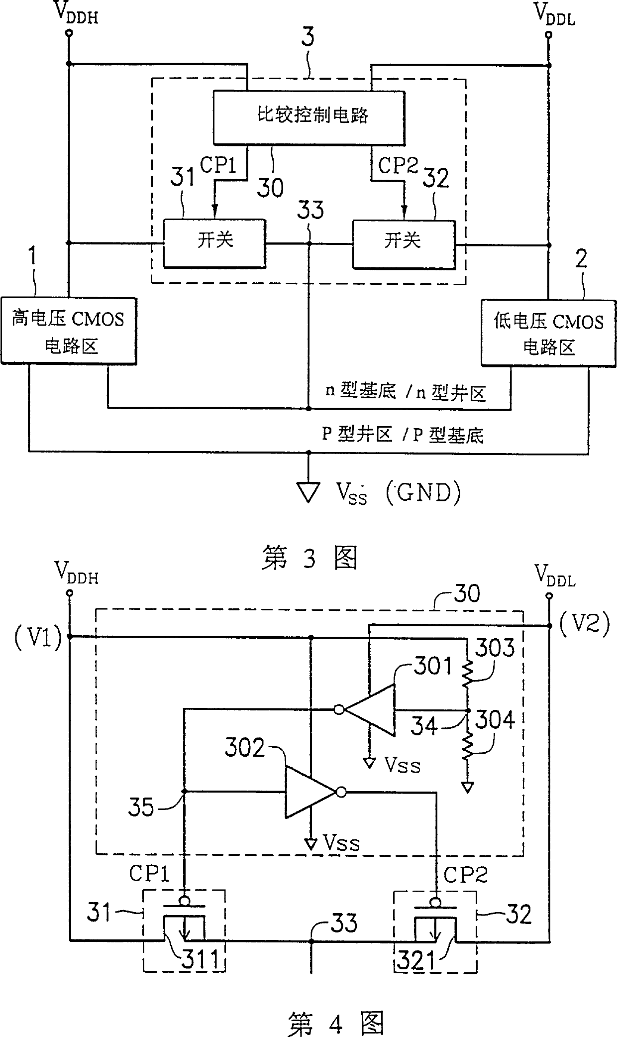
[0034] FIG. 4 is a circuit diagram of the first preferred embodiment of the latch protection circuit of FIG. 3. FIG. In Figure 4, the comparison control circuit 30 includes two inverters 301 and 302, and two resistors 303 and 304. Among them, the inverter 301 is through V DDH With V SS The power supply line provides power, and the inverter 302 passes through the V DDL With V SS The power supply line provides power. Resistors 303 and 304 are connected in series by V DDH With V SS Between the power supply lines, the resistors 303 and 304 form a circuit node 34. The inverter 301 is connected to the circuit contact 34 with its input end, and is connected to the input end of the inverter 302 with its output end, which is the circuit contact 35. The output terminals of the inverter 301 and the inverter 302 respectively output control signals CP1 and CP2.
[0035] The switch circuits 31 and 32 shown in FIG. 4 are implemented by pMOS transistors 311 and 321, respectively. Among them, the ...
no. 2 example
[0041] Figure 5 is a circuit diagram of the second preferred embodiment of the latch protection circuit of Figure 3; In Fig. 5, the comparison control circuit 30 includes two inverters 305 and 306, and four resistors 307, 308, 309, 310 and so on. Among them, the inverter 305 passes through V DDH With V SS The power supply line provides power, and the inverter 306 passes through the V DDL With V SS The power supply line provides power. The resistors 307 and 304 are connected in series with the output terminal of the inverter 306 and V SS Between the power supply lines, the resistors 303 and 304 form a circuit contact 36, and the inverter 301 is connected to the circuit contact 36 with its input terminal. The resistors 309 and 310 are connected in series with the output terminal of the inverter 305 and V SS Between the power supply lines, the resistors 303 and 304 form a circuit contact 37, and the inverter 306 is connected to the circuit contact 37 with its input terminal. The outp...
no. 3 example
[0049] FIG. 6 is a circuit diagram of the third preferred embodiment of the latch protection circuit of FIG. 3. FIG. In FIG. 6, the comparison control circuit 30 includes a differential amplifier 331, that is, two inverters 332 and 333, and so on. Among them, the differential amplifier 331 and the inverter 332 are connected via V DDL With V SS The power supply line provides power, and the inverter 333 passes through the V DDH With V SS The power supply line provides power. The differential amplifier 331 is connected to V with an inverting input terminal DDL Power supply line, connect to V with non-inverting input terminal DDH Power supply line. The differential amplifier 331 is connected to the input terminal of the inverter 332 with its output terminal, and the inverter 332 is connected to the input terminal of the inverter 333 with its output terminal. Accordingly, the output terminal of the inverter 332 outputs the control signal CP1, and the output terminal of the inverter 333...
PUM
 Abstract
Description
Claims
Application Information
 - Generate Ideas
- Intellectual Property
- Life Sciences
- Materials
- Tech Scout
- Unparalleled Data Quality
- Higher Quality Content
- 60% Fewer Hallucinations
Browse by: Latest US Patents, China's latest patents, Technical Efficacy Thesaurus, Application Domain, Technology Topic, Popular Technical Reports.
© 2025 PatSnap. All rights reserved.Legal|Privacy policy|Modern Slavery Act Transparency Statement|Sitemap|About US| Contact US: help@patsnap.com