Electron tube

A technology of electron tubes and electrons, applied in the field of electron tubes, can solve problems such as the reduction of the output of photomultiplier tubes and the deterioration of the sensitivity of the photoelectric surface

Inactive Publication Date: 2005-04-27
HAMAMATSU PHOTONICS KK
0 Cites 7 Cited by

AI-Extracted Technical Summary

Problems solved by technology

[0004] However, in conventional photomultiplier tubes, the sensitivity of the photoelectric surface deteriorates w...

Abstract

To prevent the deterioration in sensitivity of the photoelectric surface (20) of an electron tube and maintain stable output for a long time, an ion confinement electrode (22) and an ion trap electrode (23) are provided between the photoelectric surface (20) and a dynode (24a) of a first stage. The potential of the ion confinement electrode (22) is set higher than that of the dynode (24a) of the first stage, while the potential of the ion trap electrode (23) is set equal to or higher than that of the photoelectric surface (20) and lower than that of the dynode (24a) of the first stage. Since the feedback to the photoelectric surface (20) of the positive ions generated in the vicinity of the dynode (24a) of the first stage can be effectively suppressed, the sensitivity of the photoelectric surface (20) is prevented from decreasing, and stable output is maintained for a long time.

Application Domain

Multiplier circuit arrangementsMutiple dynode arrangements

Technology Topic

PhysicsIon trap +4

Image

  • Electron tube
  • Electron tube
  • Electron tube

Examples

  • Experimental program(1)

Example Embodiment

[0023] Hereinafter, a preferred embodiment of the photomultiplier tube of the present invention will be described together with the drawings. In the description of the drawings, the same reference numerals are given to the same elements, and repeated descriptions are omitted. In addition, the dimensional ratios of the drawings and the illustrated components are not necessarily the same.
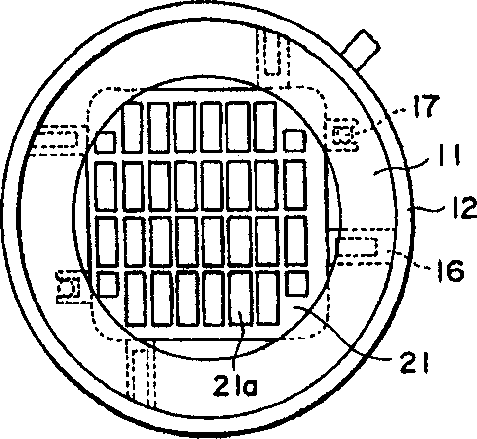
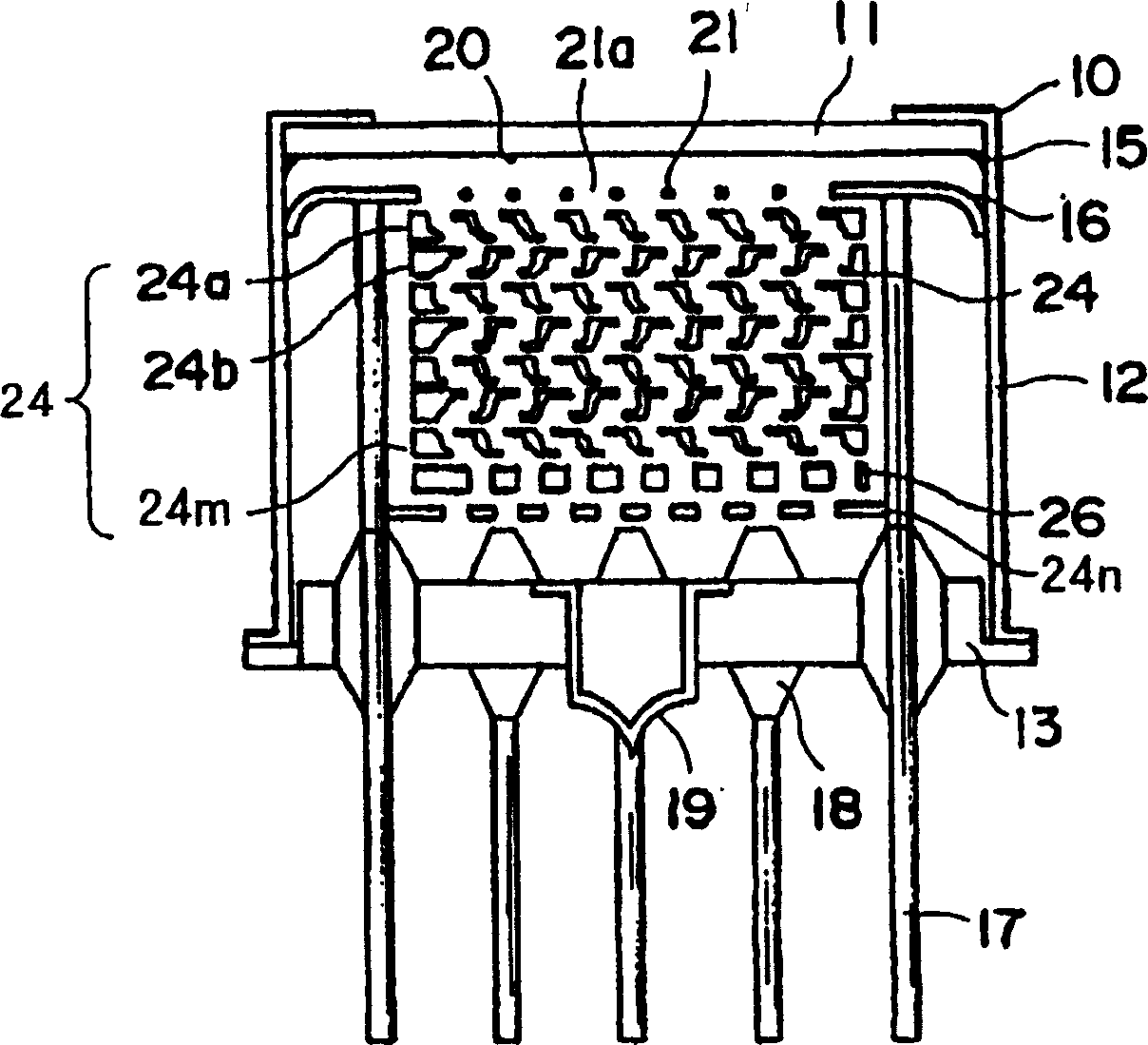
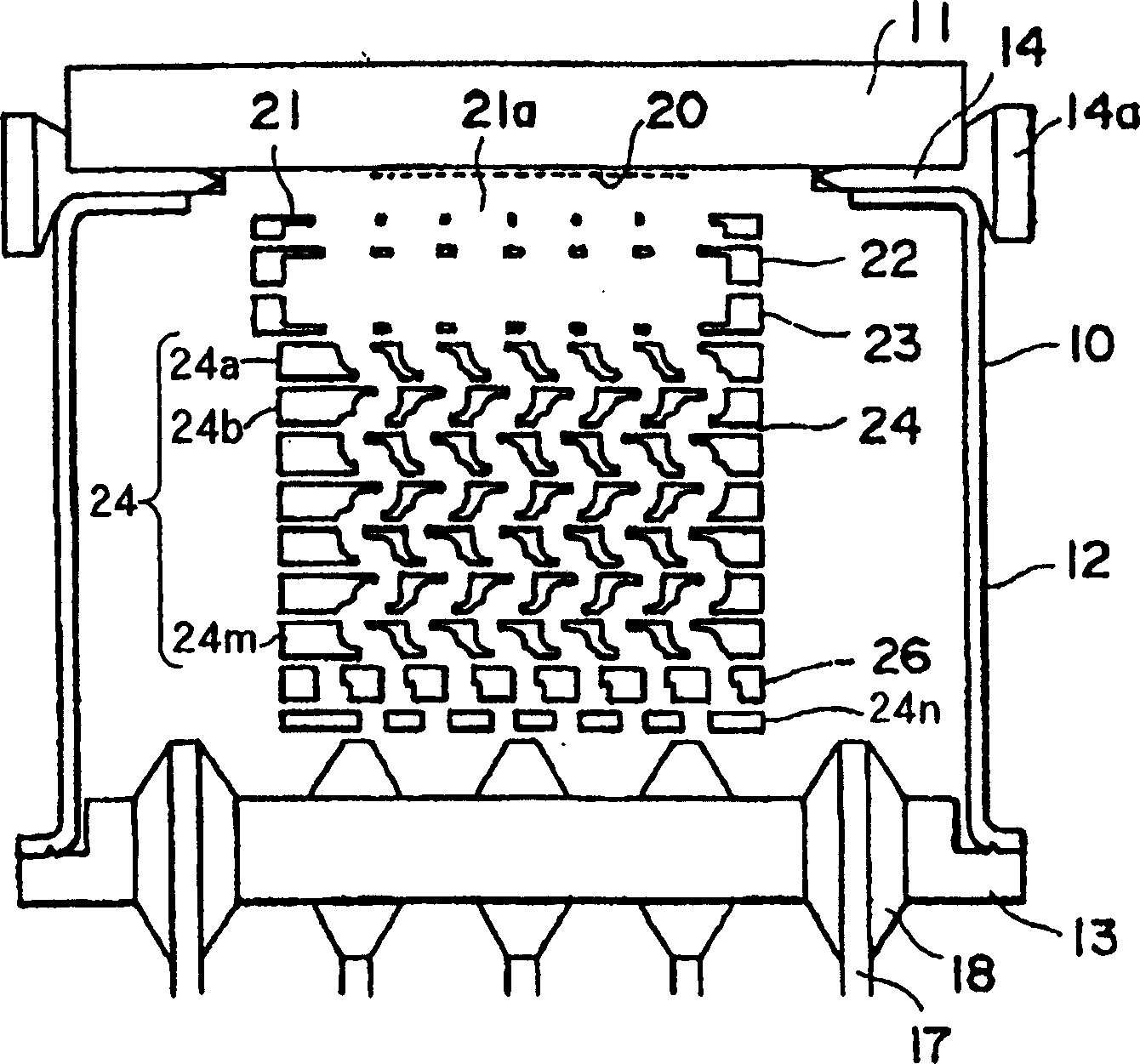
[0024] figure 2 It is a cross-sectional view of a photomultiplier tube related to the embodiment of the present invention. An electron multiplier 24 composed of multi-stage multiplier electrodes 24a-24n is arranged inside the vacuum vessel 10 to form the photomultiplier tube. The vacuum vessel 10 is formed by the following parts: a circular light-receiving panel 11 that receives incident light; arrangement A cylindrical metal side tube 12 on the outer peripheral portion of the light receiving panel 11 and a circular stem 13 constituting the base portion.
[0025] A semiconductor photoelectric surface 20 made of GaAs is formed on the inner lower surface of the light receiving panel 11, and the potential is maintained at 0 volts. In order to prevent the photoelectric surface 20 made of GaAs formed from being thermally damaged during assembly, the light receiving panel 11 and the metal side tube 12 are joined by the cold seal of the indium seal 14, and the outside is supported by the support ring 14a.
[0026] A metal channel type multiplier electrode having a secondary electron emission surface is laminated in seven stages on a predetermined portion of a square plate-shaped metal surface to form an electron multiplier 24. A plurality of electron multiplying holes are formed on the multiplier electrodes 24a-24m of each stage, and these electron multiplying holes are arranged in a slit shape. In addition, the anode electrode 26 and the final-stage dynode 24n are sequentially arranged below these stacked dynodes 24a-24m. The last-stage dynode 24n is a dynode having slits formed in a square metal plate-shaped body. The slits are arranged so that the slits are located directly under the grid of the anode electrode 27, and the slits are arranged to be directly below the grid of the anode electrode 27. The electron multiplying surface between the slits is located directly below the slit of the anode electrode 26. By arranging the last-stage dynode 24n on the rear stage of the anode electrode 26, the anode electrode 26 can be used to read the reflected secondary electrons from the last-stage dynode 24n.
[0027] The focusing electrode 21 having the electron focusing portion 21a having a plurality of openings formed in a slit shape is arranged between the photoelectric surface 20 and the first-stage multiplier electrode 24a. The focusing electrode 21 is maintained at the same potential as the photoelectric surface 20, thereby utilizing the influence of the electron focusing portion 21a, the photoelectrons emitted from the photoelectric surface 20 are focused and incident on the first-stage multiplier electrode 24a Within the specified area.
[0028] As a feature of this embodiment, the ion confinement electrode 22 and the ion trap electrode 23 are arranged between the focusing electrode 21 and the first-stage dynode 24a.
[0029] image 3 This is a perspective view showing the opening structure of the focusing electrode 21, the ion confinement electrode 22, and the ion trap electrode 23 in a cutaway view. The ion confinement electrode 22 and the ion trap electrode 23 also correspond to the slit-shaped opening of the focusing electrode 21 constituting the electron focusing portion 21a. A plurality of openings are formed in a slit shape. also, image 3 Structures other than openings such as structures for stacking and supporting contact terminals and electrodes are omitted.
[0030] The pin 17 that is connected to the external voltage terminal and supplies a predetermined voltage to the focusing electrode 21, each multiplier electrode 24, ion confinement electrode 22, ion trap electrode 23, etc. penetrates through the stem 13 that becomes the base, and is made of tapered sealing glass 18 Fix each pin 17 to the stem 13.
[0031] Figure 4 The potentials set to the ion confinement electrode 22, the ion trap electrode 23, the first-stage multiplier electrode 24a, and the second-stage multiplier electrode 24b are shown in FIG. The potential of the focusing electrode 21 is 0 volts which is the same potential as the photoelectric surface 20, and 94.1 volts and 188.2 volts are applied to the first-stage multiplier electrode 24a and the second-stage multiplier electrode 24b, respectively. In contrast to this, the potential of the ion trap electrode 23 is set to 0 volts, which is the same potential as the photoelectric surface 20, and 188.2 volts higher than the first-stage multiplier electrode 24a is applied to the ion confinement electrode 22. Regarding the potential of the ion confinement electrode 22 in the present embodiment, it is set to be equal to the second group of the multiplier electrode 24b. Therefore, it is possible to provide a potential that does not require an increase in the number of pins 17.
[0032] Figure 4 A calculation example of the positive ion orbits generated in the electron multiplier 24 when the potential of each electrode is set in this way is shown in FIG. Regarding the mechanism of generating positive ions that cause ion feedback, it can be presumed that the gas molecules adsorbed on the secondary electron emission surface of the first-stage multiplier electrode 24a are caused by photoelectrons incident on the first-stage multiplier electrode 24a. When emitted, photoelectrons or secondary electrons are positively ionized by colliding with the gas molecules.
[0033] In the above-mentioned electrode structure, in the vicinity of the first-stage dynode 24a ( Figure 4 The positive ions generated in the area A) in the middle are suppressed by the ion confinement electrode 22 in potential, and finally absorbed by the ion trap electrode 23, and the other part is absorbed by the first-stage multiplier electrode 24a itself, so the positive ions cannot reach the photoelectric surface.
[0034] In addition, considering the electron flow, it can be assumed that the number of square positive ions near the multiplier electrode after the second stage is large. Figure 4 Shows in the vicinity of the second-stage multiplier electrode 24b ( Figure 4 The calculation example of the trajectory of the positive ions generated in the area B) in the middle. These positive ions are absorbed by the dynode of the previous stage, and therefore, in this case, by the first stage dynode 24a, or by the second stage dynode 24b absorbs itself. Therefore, it can be inferred that even in the existing photomultiplier tube, the positive ions generated near the second and subsequent stages of the multiplier electrode do not contribute to ion feedback and the deterioration of the photosurface caused by it. The condition that the potential of 22 is set higher than the potential of the first-stage multiplier electrode 24a can obtain a sufficient effect of suppressing ion feedback.
[0035] Compare the time-dependent change characteristics of the relative output of the photomultiplier tube with the structure shown in the above-mentioned embodiment with the conventional photomultiplier tube with GaAs semiconductor photosurface without ion confinement electrode and ion trap electrode, and Shown in Figure 5 in. The output of the existing device drops to 55% after 100 hours. Unlike this, the improved device of the present invention still has 98% after 100 hours, and there is no output drop caused by the deterioration of the photoelectric surface. , Can achieve very stable performance.
[0036] The present invention is not limited to the above-mentioned embodiment, and can be applied to various types of electron tubes. Here, the so-called electron tube in the present invention is a device having a structure with a photoelectric surface in the internal space separated by the light receiving panel, the side tube, and the stem. In addition to the photomultiplier tube described above, it also includes an image. Tube and so on. The so-called shift tube is the photoelectric conversion of the incident optical image on the photoelectric surface to convert it into a photoelectric image. After the photoelectric image is accelerated and imaged by the electronic lens system, the photoelectric image is multiplied by the electron multiplier and then incident on the phosphor surface. An electron tube that reproduces as an optical image.
[0037] In the above embodiment, a metal channel type multiplier electrode having a plurality of electron multiplying holes arranged in slits on each stage of the multiplier electrode is used. However, a metal channel having a plurality of electron multiplying holes may also be used Type multiplier electrode. In this case, such as Figure 6 As shown in the figure, the opening structures of the focusing electrode, ion confinement electrode, and ion trap electrode are also made into matrix-like openings corresponding to the dynodes. Furthermore, for multiplier electrodes that do not have multiple electron multiplying holes in the multiplier electrodes of each stage, and for example, multipliers other than metal channel types such as multiplier electrodes with secondary electron emission surfaces formed on predetermined portions of the ceramic surface The same function and effect can be obtained with the electrode.
[0038] In addition, the focusing electrode is used in the above-mentioned embodiment, but the same function and effect can be obtained even when the focusing electrode is not used such as a photomultiplier tube or a picture tube using a microchannel plate. Such as Figure 7 As shown in the figure, the microchannel plate 25 is a plate formed by bundling fine glass tubes 250 with the inner wall as the secondary electron emission surface. One surface (electron incident surface) 25a faces the photoelectric surface and the other The plate is arranged so that one surface (electron emission surface) 25b faces the anode electrode. The microchannel plate 25 is a multiplier electrode that multiplies incident electrons by repeating the collision of electrons on the inner wall of the glass tube 250 and the emission of secondary electrons. The electron incident surface 25a is applied to the present invention as the electron incident portion of the electron multiplier.
[0039] Possibility of industrial use
[0040] In the electron tube of the present invention, the photomultiplier tube can be widely used in medical devices, analytical devices, industrial measuring devices, etc., as an optical analysis device that uses absorption, reflection, and polarization of a specific wavelength to analyze various substances. Furthermore, it can be applied to X-ray, star observation, solar observation, environmental measurement inside and outside the atmosphere, and auroral observation.

PUM

no PUM

Description & Claims & Application Information

We can also present the details of the Description, Claims and Application information to help users get a comprehensive understanding of the technical details of the patent, such as background art, summary of invention, brief description of drawings, description of embodiments, and other original content. On the other hand, users can also determine the specific scope of protection of the technology through the list of claims; as well as understand the changes in the life cycle of the technology with the presentation of the patent timeline. Login to view more.
Why Eureka
Try Eureka