Supercharge Your Innovation With Domain-Expert AI Agents!

Process for preparing MOS transistor

A manufacturing process, semiconductor technology, applied in the direction of semiconductor/solid-state device manufacturing, electrical components, circuits, etc., can solve the problems of component stability, reduce product qualification rate, change the electrical characteristics of components, etc., to increase the qualification rate and improve stability performance, and the effect of reducing the amount of loss

Inactive Publication Date: 2005-06-22
MACRONIX INT CO LTD
View PDF0 Cites 0 Cited by
  • Summary
  • Abstract
  • Description
  • Claims
  • Application Information

AI Technical Summary

Problems solved by technology

If the thickness variation of the gate oxide layer in the above tempering process is about 6 Å to 10 Å, when the thickness of the gate oxide layer is 100 Å, the thickness change rate of the gate oxide layer is only about 10%. , the element still has sufficient stability at this time; however, when the thickness of the gate oxide layer drops to 25 Å, the thickness change rate of the gate oxide layer increases to about 50%, which will cause considerable damage to the stability of the element. big impact
[0005] In addition, during the tempering process of the known method, the dopant impurities located in the gate are easily diffused into the underlying substrate due to the double influence of high temperature and polysilicon grain size, thereby changing the electrical characteristics of the element, and May cause component failure and reduce product yield

Method used


Image

  • Process for preparing MOS transistor
  • Process for preparing MOS transistor
  • Process for preparing MOS transistor

Examples


Embodiment Construction

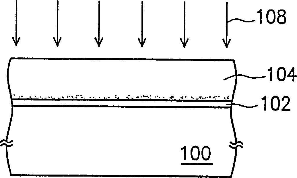
[0023] Figure 1 to Figure 2 Shown is a schematic diagram of a metal oxide semiconductor transistor process in a preferred embodiment of the present invention. Please refer to figure 1 First, a substrate 100 is provided, and then a gate dielectric layer 102 and a polysilicon layer 104 are sequentially formed on the substrate 100 , wherein the material of the gate dielectric layer 102 includes silicon dioxide.

[0024] Next, please refer to figure 2 , implanting nitrogen ions 108 into the connection between the polysilicon layer 104 and the gate dielectric layer 102 , wherein the implantation dose and energy used need to be adjusted according to the actual situation.

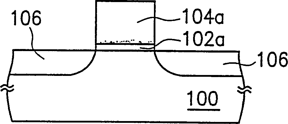
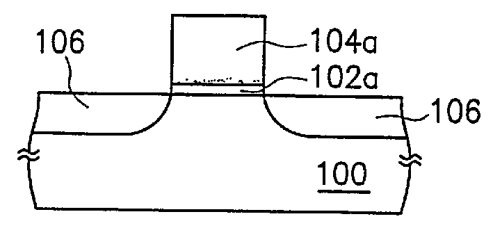
[0025] A tempering step is then performed to enlarge the grains in the polysilicon layer 104 . Next, a photolithographic etching process is performed to pattern the polysilicon layer 104 to form the gate 104a. Next, an ion implantation step is performed to form source / drain regions 106 in the substrates on b...


PUM


Abstract

A metal oxide semiconductor transistor manufacturing process is to sequentially form a gate dielectric layer and a polysilicon layer on a substrate, and then implant nitrogen ions into the contact area between the polysilicon layer and the gate dielectric layer. Next, a tempering step is performed to make the polysilicon grains in the polysilicon layer larger, and then the polysilicon layer is patterned to form a gate, and doping impurities are implanted into the substrate on both sides of the gate to form a source / drain pole.

Description

technical field [0001] The invention relates to a semiconductor process, and in particular to a manufacturing process of a metal oxide semiconductor transistor (MOS Transistor). Background technique [0002] The known MOS process is to sequentially form a gate oxide layer and a polysilicon layer on a substrate, and then perform a tempering step to make the polysilicon grains in the polysilicon layer larger, then pattern the polysilicon layer to form a gate, and then Doping impurities are doped into the substrate on both sides of the gate to form source / drain. [0003] However, during the tempering process of the known MOS process, the polysilicon located near the newly grown grain boundary (Grain Boundary) will react with the gate oxide layer to generate volatile SiO, which will consume the gate near the grain boundary. Oxide layer, resulting in uneven thickness of the entire gate oxide layer. [0004] When the degree of component integration gradually increases, the thick...

Claims


Application Information

Patent Timeline
Patent Type & Authority Patents(China)
IPC IPC(8): H01L21/336
Inventor 赖汉昭林宏穗卢道政
Owner MACRONIX INT CO LTD
Features
  • R&D
  • Intellectual Property
  • Life Sciences
  • Materials
  • Tech Scout
  • Unparalleled Data Quality
  • Higher Quality Content
  • 60% Fewer Hallucinations
Learn More