Dielectric layer reetching method

A dielectric layer and etch-back technology, which is applied in the manufacture of circuits, electrical components, semiconductors/solid-state devices, etc., can solve the problem of uneven thickness of the dielectric layer and achieve the effect of improving the problem of uneven thickness of the dielectric layer

Inactive Publication Date: 2006-01-25
NAN YA TECH
View PDF0 Cites 2 Cited by
  • Summary
  • Abstract
  • Description
  • Claims
  • Application Information

AI Technical Summary

Problems solved by technology

[0005] In view of this, the main purpose of the present invention is to provide a dielectric layer etching back method to replace the CMP manufacturing process, which can improve the uneven thickness of the dielectric layer and provide a better planarized structure

Method used


Image

  • Dielectric layer reetching method
  • Dielectric layer reetching method
  • Dielectric layer reetching method

Examples


Embodiment Construction

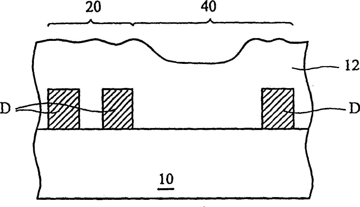
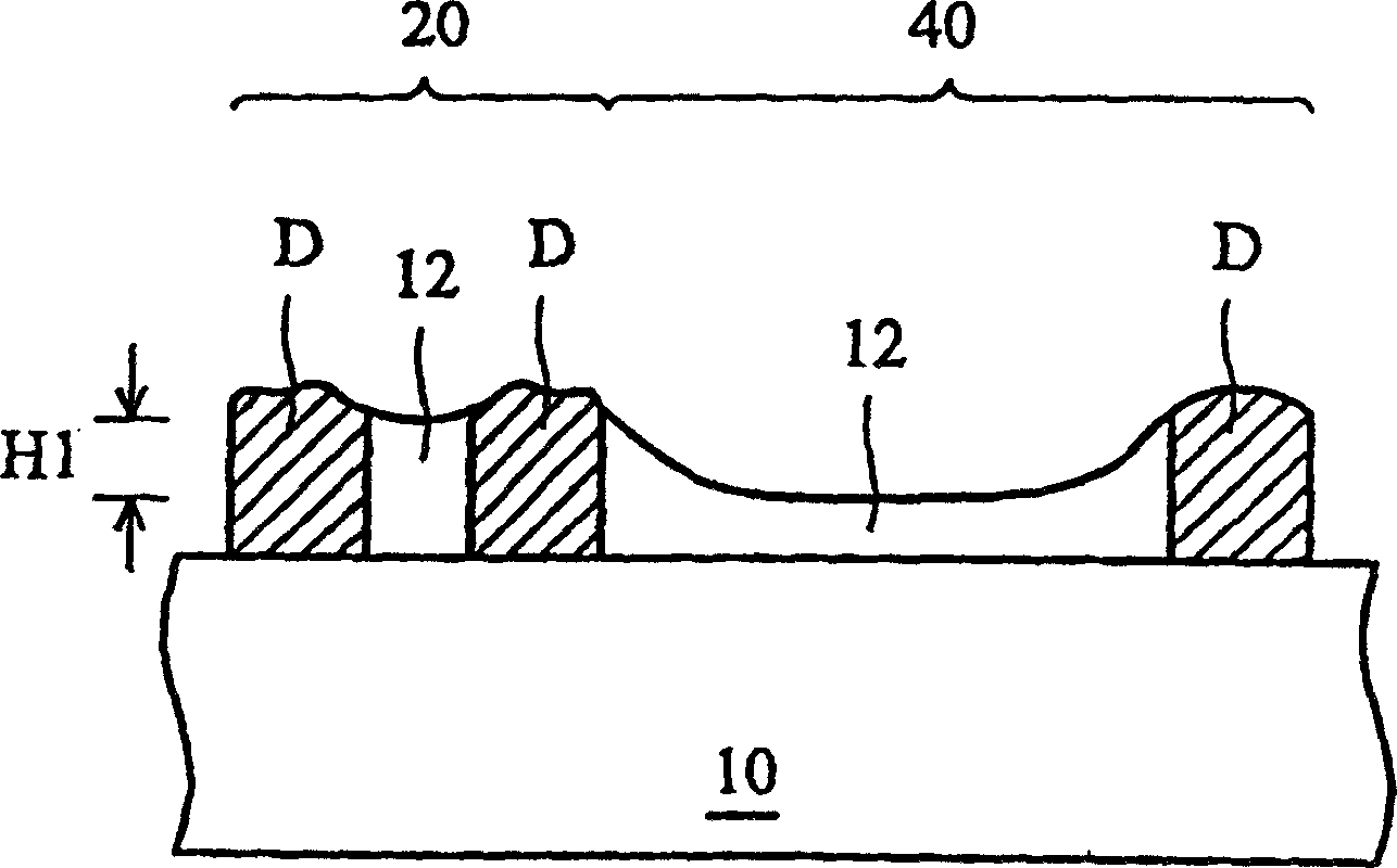
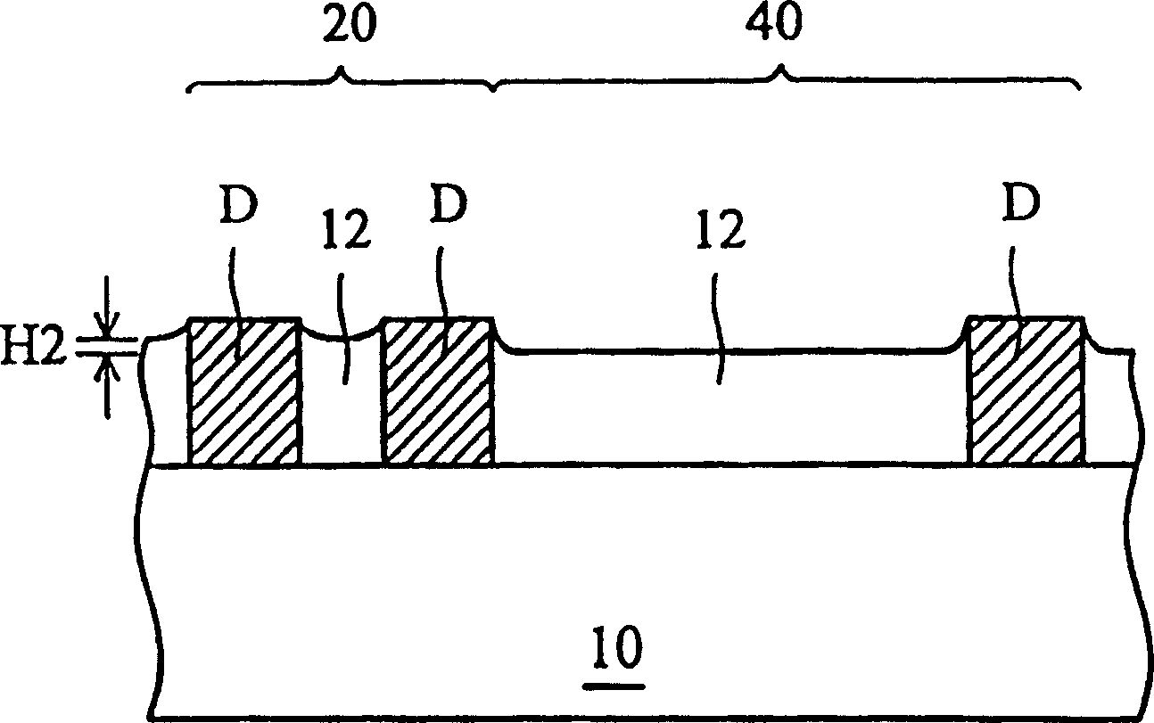
[0017] In this embodiment, the ILD layer is planarized according to the method of the present invention to provide a better planarized structure. Such as figure 1 As shown, a semiconductor substrate 10 is provided, with a plurality of elements D distributed in a sparse area 40 with a small number of elements and a dense area 20 with a large number of elements. The elements D are, for example, MOS transistors, capacitor structures (capacitor ) or other logic components (logic devices), while the surface of component D is made of silicon nitride (Si 3 N 4 ), polysilicon (poly-silicon), amorphous silicon (amorphoussilicon), metal or metal nitride and other non-oxygen (Oxygen free) materials. Next, a dielectric layer material is formed to cover the element D in the element sparse region 40 and the element dense region 20, wherein the dielectric layer material is formed of an oxygen-containing (oxygen contained) material, For example, silicon dioxide, doped silicon dioxide (BSG,...


PUM


Abstract

The invention method is suitable to working procedure for evening inter layer dielectric (ILD) and inter metal dielectric (IMD) in flow for manufacturing semiconductor parts so as to improve the issue of inconsistence dielectric thickness after chemically machinery grinding. The method includes following steps. A semiconductor substrate possessing multiple components or patternized metal conducting wire is provided. A dielectric layer is formed to cover components or metal conducting wires uniformly. Etch back procedure is carried out by using technology of reactivity ion etching (RIE) with etching gas containing C5H3, CHF3 and Ar. The said etching procedure is stopped on the components or patternized metal conducting wire in order to form an even dielectric layer between components and wires.

Description

technical field [0001] The invention relates to a manufacturing process of a semiconductor element, especially a manufacturing process technology for improving the uneven thickness of a dielectric layer after a planarization process. One-pass etching technology is used to optimize the proportion of etching gas used to improve the dielectric layer thickness after etching. The semiconductor manufacturing process that achieves the purpose of flattening the electrical layer can specifically improve the problem of inconsistent thickness of the dielectric layer after chemical mechanical polishing, especially suitable for inter-layer dielectric (ILD) and metal layers The planarization manufacturing process of the dielectric layer (inter-metal dielectric; IMD). Background technique [0002] With the complexity of integrated circuit structures, the number of structural layers formed on a semiconductor substrate (such as a silicon substrate) is increasing. The additional film layer f...

Claims


Application Information

Patent Timeline
Patent Type & Authority Patents(China)
IPC IPC(8): H01L21/311
Inventor 孙玉琪黄则尧
Owner NAN YA TECH
Why Eureka
Try Eureka