Broadband absorbing material based on frequency selective surface and sandwich structure design and preparation method thereof

A frequency-selective surface and interlayer structure technology, applied in the field of wave-absorbing materials, can solve the problems of limited electromagnetic wave attenuation ability and single form, and achieve the effects of adjustable and controllable wave-absorbing frequency, widening the application field, and easy operation

Inactive Publication Date: 2018-02-23
NORTHWESTERN POLYTECHNICAL UNIV
View PDF14 Cites 9 Cited by
  • Summary
  • Abstract
  • Description
  • Claims
  • Application Information

AI Technical Summary

Problems solved by technology

At the same time, the FSS in this type of absorber is mainly carbon powder and other materials, and its loss mechanism is conductance loss, which has a single form and has limited ability to attenuate electromagnetic waves.

Method used


Image

  • Broadband absorbing material based on frequency selective surface and sandwich structure design and preparation method thereof
  • Broadband absorbing material based on frequency selective surface and sandwich structure design and preparation method thereof
  • Broadband absorbing material based on frequency selective surface and sandwich structure design and preparation method thereof

Examples


preparation example Construction

[0038] In the field of low temperature (<400°C) application, the preparation method of the absorbing material includes: (1) When the dielectric layer is resin / polymer: according to the structural design plan, firstly use the compression molding process to prepare the upper and lower layers with a specific thickness. The lower medium layer, and then use the brushing process to periodically arrange and paste the FSS film on the inner surface of the medium layer, and finally achieve three-layer adhesion; (2) When the medium layer is a fiber-reinforced resin-based composite material / polymer-based composite material : Taking the two-dimensional (fiber cloth layer) prefabricated body structure as an example, according to the structural design plan, first determine the thickness of the upper and lower medium layers and the number of fiber cloth layers, and then carry out fiber cloth layering. Then the FSS film is periodically arranged on the surface of the corresponding layer of fiber...

Embodiment 1

[0042] (1) 300 mg of graphene oxide was placed in 300 mL of ethylene glycol solution for ultrasonic dispersion for 3 h to prepare a 1 mg / mL graphene oxide dispersion.

[0043] (2) Pour the uniform graphene dispersion into a polytetrafluoroethylene reactor, treat at 180° C., and keep warm for 12 hours.

[0044] (3) Take 10 mL of the hydroheated dispersion and slowly drop it into a vacuum filter bottle, dry it naturally, and remove the graphene film from the microporous filter. Repeat the above operations to prepare a series of identical graphene films.

[0045] (4) Put the composite film obtained by the above treatment in a muffle furnace (argon atmosphere), heat treatment temperature 600° C., keep it warm for 1 hour, and then cool down with the furnace.

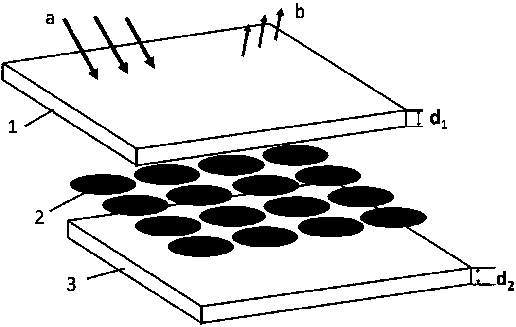
[0046] (5) The upper and lower dielectric layers are all selected as molded epoxy resin boards, d 1 = 2.2mm, d 2 = 1.2 mm. The graphene film is pressed as figure 1 It is periodically coated on the lower dielectric board,...

Embodiment 2

[0049] (1) 300 mg of graphene oxide was placed in 300 mL of ethylene glycol solution for ultrasonic dispersion for 3 h to prepare a 1 mg / mL graphene oxide dispersion.

[0050] (2) Pour the uniform graphene dispersion into a polytetrafluoroethylene reactor, treat at 180° C., and keep warm for 12 hours.

[0051] (3) Take 10 mL of the hydroheated dispersion and slowly drop it into a vacuum filter bottle, dry it naturally, and remove the graphene film from the microporous filter. Repeat the above operations to prepare a series of identical graphene films.

[0052] (4) Put the composite film obtained by the above treatment in a muffle furnace (argon atmosphere), heat treatment temperature 800° C., keep it warm for 1 hour, and then cool down with the furnace.

[0053] (5) Pour polydimethylsiloxane resin (PDMS) into a mold of 180mm*180mm*3mm, and cure at high temperature to obtain d 1 = 3mm PDMS dielectric layer. The graphene film is pressed Figure 1 The arrangement shown is pla...


PUM


Abstract

The invention relates to a broadband absorbing material based on a frequency selective surface and sandwich structure design and a preparation method thereof. On the basis of combination of a frequency selective surface and a sandwich structure, the advantage of widening the absorbing band of the frequency selective surface is utilized and the frequency selective surface is protected from being corroded by a high-temperature aerobic environment. According to different environmental usage requirements like the temperature or bearing requirement, different dielectric layer materials are selectedpreferably and the corresponding preparation processes are optimized, so that the application field of the absorbing material is widened. Besides, the intermediate electromagnetic wave loss layer isa frequency selective surface film based on multi-loss-mechanism coordination with compatibility of conductivity losses and polarization losses instead of the traditional frequency selective surface.On the basis of the macro-scale structural design and micro-scale frequency selective surface film optimization and regulation, the frequency width of the reflection loss <-10dB of the material is 8 to 18 GHz. Moreover, the preparation method of the broadband absorbing material is simple and has high designability; the performances are stable; the applicability is high; and the broadband absorbingmaterial and the preparation method thereof have the development prospects.

Description

technical field [0001] The invention belongs to the field of wave-absorbing materials, and relates to a broadband wave-absorbing material designed based on a frequency selective surface and a sandwich sandwich structure and a preparation method thereof. Background technique [0002] With the rapid development of electronic communication, the electromagnetic environment is becoming increasingly complex, and electromagnetic radiation has become a new type of pollution after water pollution, air pollution and noise pollution. Electromagnetic radiation not only interferes with the normal operation of electronic equipment and instruments, but also endangers human health. Therefore, it is urgent to develop electromagnetic absorbing materials and absorbing structures with broadband, strong absorption and wide application range, so as to cope with electromagnetic pollution in different environments and reduce electromagnetic radiation. [0003] At present, researchers mainly carry ...

Claims


Application Information

Patent Timeline
Patent Type & Authority Applications(China)
IPC IPC(8): H05K9/00
CPCH05K9/0081
Inventor 殷小玮叶昉宋昶晴周倩韩美康成来飞张立同
Owner NORTHWESTERN POLYTECHNICAL UNIV
Why Eureka
Try Eureka