
Method for contruction of two-dimension ordered distributing silicon quantum point figurated nano structure
A technology of silicon quantum dots and nanostructures, which is applied in the field of patterned nanostructures of high-density silicon quantum dots, can solve the problems of controllability of nanometer quantum dots size and difficulty in patterning distribution order, and achieve strong controllability Effect
- Summary
- Abstract
- Description
- Claims
- Application Information
AI Technical Summary
Problems solved by technology
Method used
Image

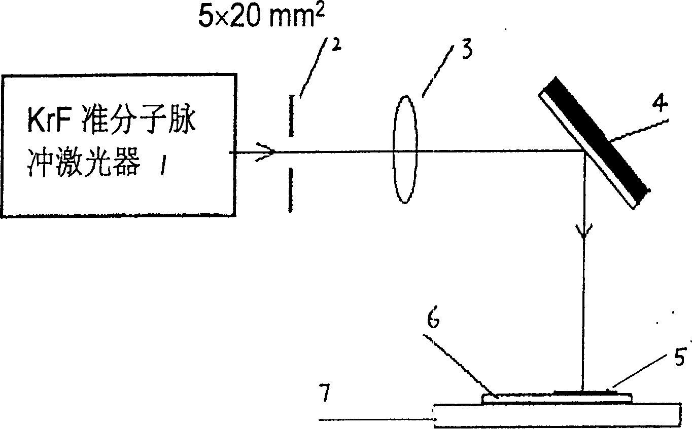
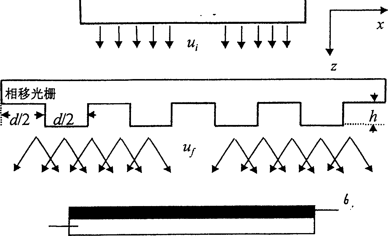
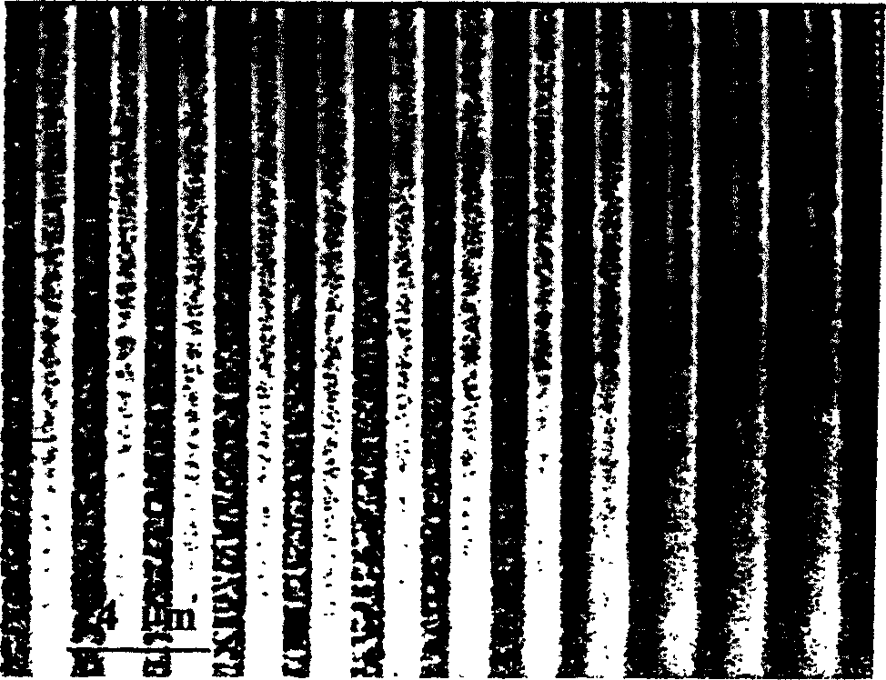
Examples
Embodiment Construction
[0024] 1. Preparation of ultra-thin amorphous silicon (a-Si) film: a-Si:H film was prepared by plasma enhanced chemical vapor deposition (PECVD). The thickness of the a-Si:H layer can be precisely controlled in the range of 1.0-10nm; the size of the quantum dots to be obtained after laser crystallization is basically consistent with the thickness of the a-Si:H layer. Similarly, we can also prepare (a-SiN X :H / a-Si:H / a-SiN X :H) Three-layer sandwich structure, which has a wider application in nanoelectronic devices.
[0025] a-Si:H film and a-SiN X :H / a-Si:H / a-SiN X :H Preparation of three-layer sandwich structure film:
[0026] Using computer-controlled plasma-enhanced chemical vapor deposition (PECVD) technology, using silane (SiH 4 ), ammonia (NH 3 ) and argon (Ar) as the reaction gas source; deposit a-Si:H film or a-SiN on single crystal silicon wafer and double-throw fused quartz or optical glass substrate X :H / a-Si:H / a-SiN X :H three-layer structure film. Concret...
PUM
 Abstract
Description
Claims
Application Information