Method for imaging processing of nanorod/nanoneedle forest structure

A processing method and nano-pillar technology, which can be applied in the fields of nano-structure manufacturing, nano-technology, nano-technology, etc., can solve the problems that limit the integrated application of nano-pillar/needle forest structure, difficult to pattern arrangement of single-layer spheres, and increase the complexity of the process. and other problems, to achieve the effect of enhancing the plasmonic oscillation of optical absorption characteristics, improving production efficiency and integration, large surface area and surface-to-body ratio

Active Publication Date: 2015-01-28
中科芯未来微电子科技成都有限公司
View PDF2 Cites 1 Cited by
  • Summary
  • Abstract
  • Description
  • Claims
  • Application Information

AI Technical Summary

Problems solved by technology

Theoretically, electrochemical wet etching technology can easily obtain the nano-forest structure, but the controllability of the structure is relatively poor, and the acid etching method also uses metal nanoparticles, which also increases the complexity of the process
The combination of nanosphere etching technology and anisotropic etching can also be used to process nanopillar / needle forest structures. However, the patterning of monolayer nanospheres requires strict control conditions, and even under strict control Under the premise of this, it is still difficult to realize the graphic arrangement of single-layer small balls in a large area
This limits the integrated application of the nanopillar / needle forest structure in specific micro-nano devices

Method used


Image

  • Method for imaging processing of nanorod/nanoneedle forest structure
  • Method for imaging processing of nanorod/nanoneedle forest structure
  • Method for imaging processing of nanorod/nanoneedle forest structure

Examples


Embodiment 1

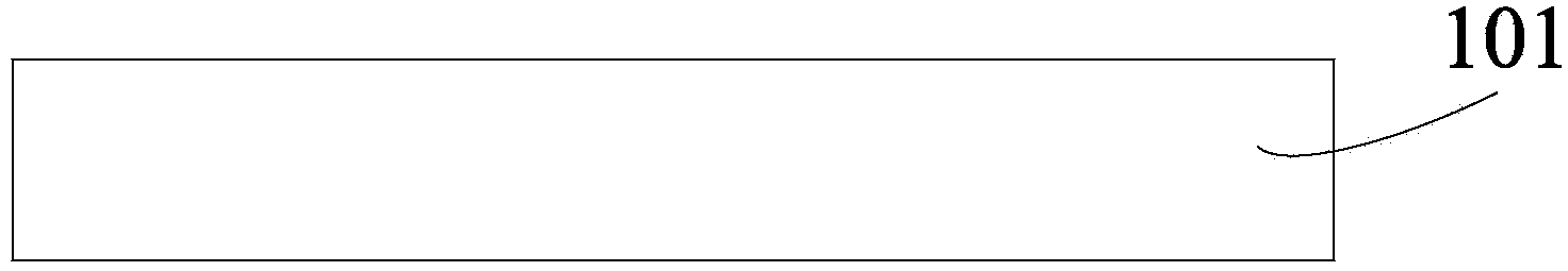
[0042] The first substrate 101 is made of silicon material, the second substrate 102 is made of silicon material, and the first substrate similar material layer 103 is the surface layer of the second substrate 102 and is also made of silicon material. The experimental methods described in the following examples are conventional methods unless otherwise specified.

[0043] a. Prepare and clean the selected first substrate 101 and second substrate 102;

[0044] Such as figure 1 , the first substrate 101 is a silicon substrate that finally obtains a nano-column / needle forest structure 401 on its surface, and the second substrate 102 is a material layer for realizing a hollow substrate, which needs to be cleaned before the experiment, specifically The cleaning process will not be repeated.

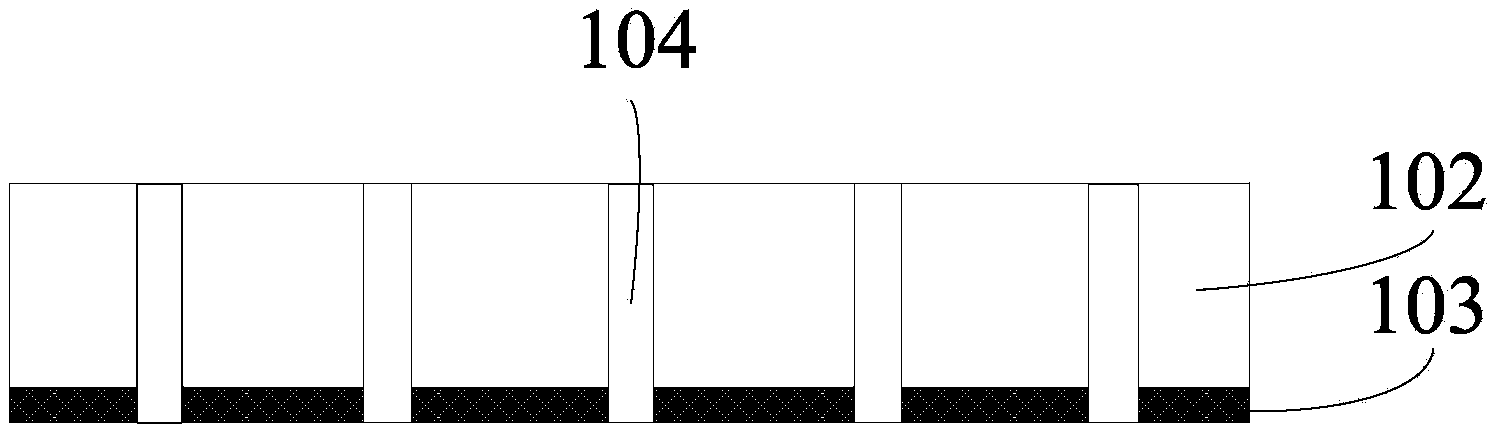
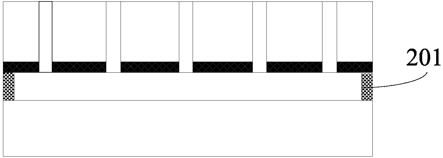
[0045] b. A first substrate-like material layer 103 similar to that of the first substrate 101 is provided on the lower surface of the above-mentioned second substrate 102, and several throu...

Embodiment 2

[0054] The first substrate 101 is made of glass material, the second substrate 102 is made of glass material, and the layer 103 of similar material to the first substrate is the surface layer of the second substrate 102 and is also made of glass material. The experimental methods described in the following examples are conventional methods unless otherwise specified.

[0055] a. Prepare and clean the selected first substrate 101 and second substrate 102;

[0056] Such as figure 1 , the first substrate 101 is a glass substrate with a nano-column / needle forest structure finally obtained on its surface, and the second substrate 102 is a material layer for realizing a hollow structure, also using glass, which needs to be cleaned before the experiment.

[0057] b. A first substrate-like material layer 103 similar to that of the first substrate 101 is provided on the lower surface of the above-mentioned second substrate 102, and several through structures 104 are arranged on the se...

Embodiment 3

[0066] The first substrate 101 is made of silicon material, the second substrate 102 is made of glass material, and the material layer 103 similar to the first substrate is made of amorphous silicon material. The experimental methods described in the following examples are conventional methods unless otherwise specified.

[0067] a. Prepare and clean the selected first substrate 101 and second substrate 102;

[0068] Such as figure 1 , the first substrate 101 is the silicon substrate on which the nano-column / needle forest structure 401 is finally obtained on the surface, and the second substrate 102 is a material layer for realizing the hollow structure, which needs to be cleaned before the experiment.

[0069] b. A first substrate-like material layer 103 similar to that of the first substrate 101 is provided on the lower surface of the above-mentioned second substrate 102, and several through structures 104 are arranged on the second substrate 102. The through structures 104...


PUM

PropertyMeasurementUnit
diameteraaaaaaaaaa
diameteraaaaaaaaaa
heightaaaaaaaaaa

Abstract

The invention relates to a method for imaging processing of a nanorod/nanoneedle forest structure. The method comprises a step (a) of cleaning a first substrate and a second substrate; a step (b) of enabling a first substrate similar material layer similar to a first substrate material to be arranged on the lower surface of the second substrate, and arranging a plurality of punchthrough structures on the second substrate so as to form a hollow substrate; a step (c) of pasting the hollow substrate to the upper surface of the first substrate so as to form a corrosion cavity between the lower surface of the hollow substrate and the upper surface of the first substrate; a step (d) of utilizing the punchthrough structures of the hollow substrate to etch the upper surface of the first substrate; and a step (e) of removing the hollow substrate from the upper surface of the first substrate, so as to obtain the nanorod/nanoneedle forest structure on the first substrate. According to the method, the limitation of an electron beam photoetching and focused ion beam etching technology in the aspect of batch processing can be overcome, the process complexity can be effectively reduced, and the imaging nanorod/nanoneedle forest structure having controllability is achieved.

Description

technical field [0001] The invention relates to a pattern processing method, in particular to a pattern processing method of a nano-column / needle forest structure, belonging to the technical field of nano-structure processing. Background technique [0002] Large-area nanopillar / needle structure, due to its structural characteristics such as large surface-to-volume ratio, large roughness, large surface area, tip, multi-pore / slit, etc., it presents super-hydrophilic / hydrophobic, enhanced plasmon oscillation, field emission, light filtering, Light absorption and other properties are often applicable to microfluidic devices, surface-enhanced Raman scattering devices, biomedical detection or functional devices, optoelectronic devices, optical sensor devices, new energy devices, etc., so it has gradually become one of the research hotspots in recent years. In many cases, the large-area, high-density nanopillar / needle structure looks like a dense forest, so it is also called the na...

Claims


Application Information

Patent Timeline
Patent Type & Authority Applications(China)
IPC IPC(8): B82B3/00B82Y40/00
Inventor 毛海央王岩唐力程雷程欧文陈大鹏
Owner 中科芯未来微电子科技成都有限公司
Why Eureka
Try Eureka