Semiconductor laser device

A laser device and semiconductor technology, applied in the field of semiconductor laser devices

Inactive Publication Date: 2006-05-31
SANYO ELECTRIC CO LTD +1
View PDF0 Cites 1 Cited by
  • Summary
  • Abstract
  • Description
  • Claims
  • Application Information

AI Technical Summary

Problems solved by technology

However, with this configuration, when the main lead frame 103 is fed a predetermined distance on the machine before the tie bars are cut, vibrations of the feed or the like cause, for example, the end portion of the first lead frame 100 to move in the direction indicated as G1 or G2. tilt up

Method used


Image

  • Semiconductor laser device
  • Semiconductor laser device
  • Semiconductor laser device

Examples


Embodiment Construction

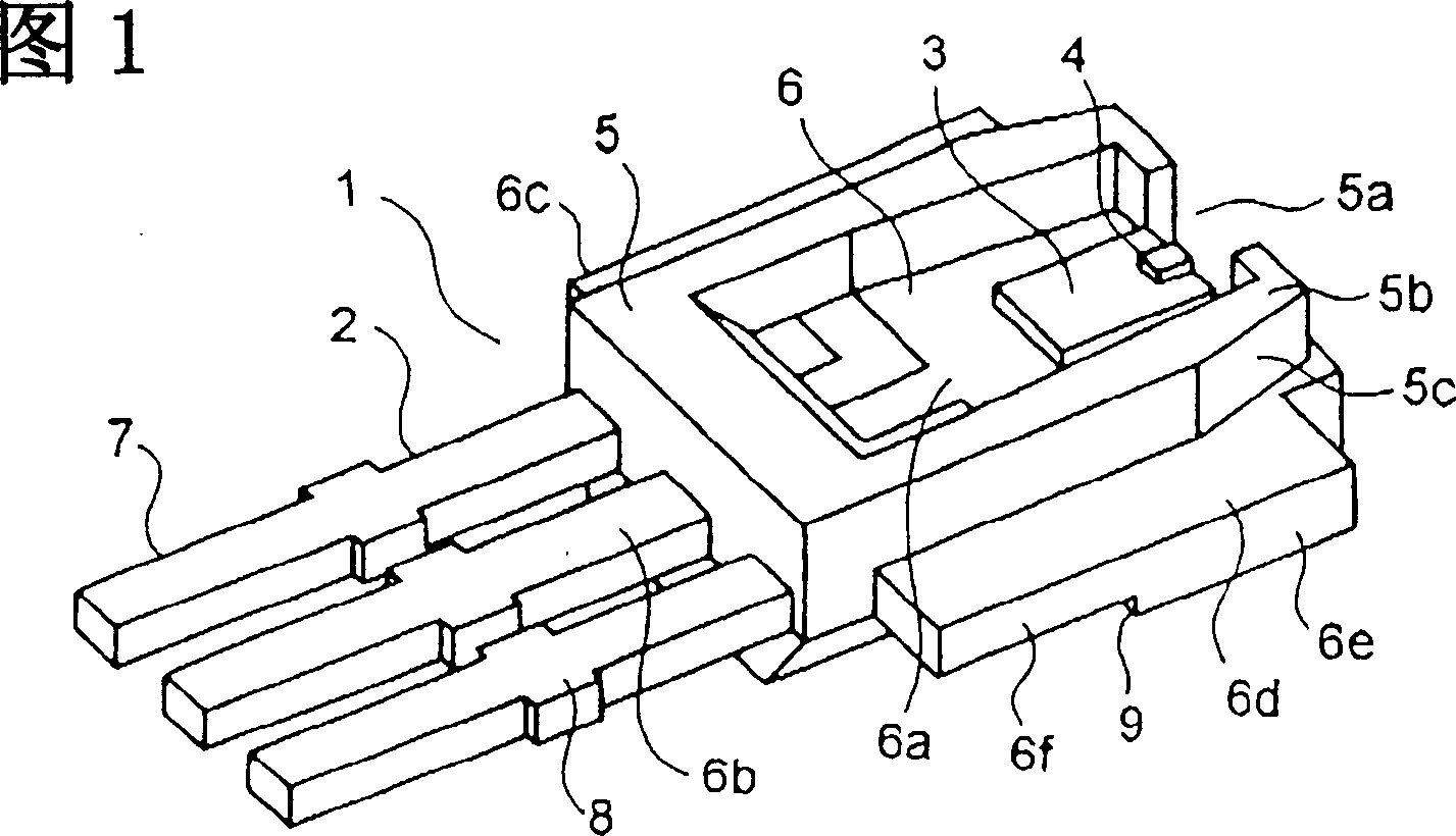
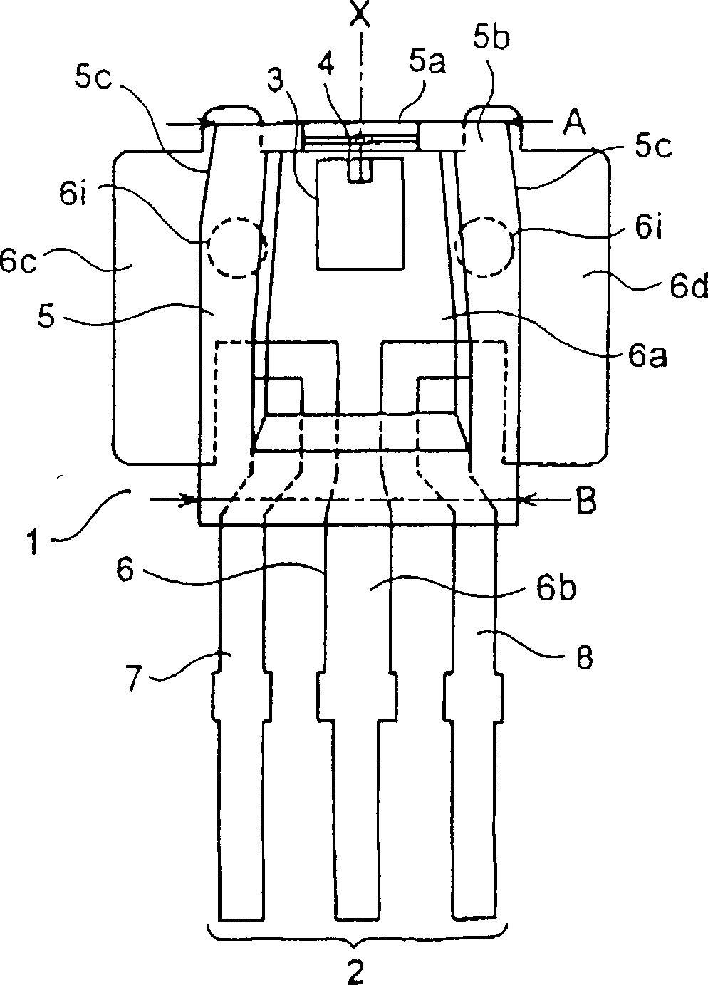
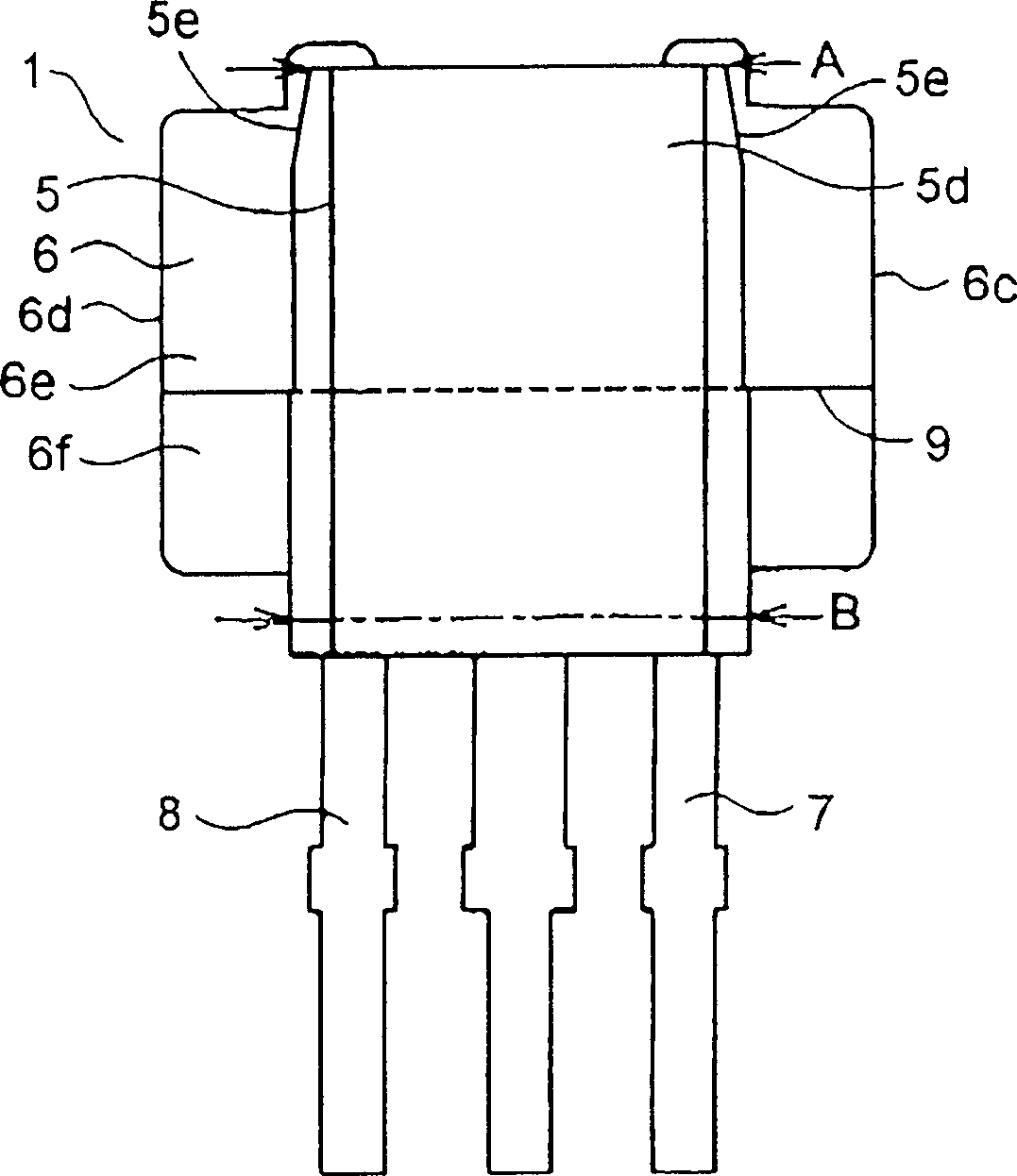
[0030] First, a first embodiment of the present invention will be described with reference to the drawings. Fig. 1 is a perspective view of a semiconductor laser device according to a first embodiment of the present invention. figure 2 is a front view of the semiconductor laser device of the first embodiment of the present invention. image 3 is a rear view of the semiconductor laser device of the first embodiment of the present invention. Figure 4 is a sectional view of the semiconductor laser device of the first embodiment of the present invention.

[0031] In the semiconductor laser device 1 of this embodiment, a submount 3 is arranged and fixed on the top surface of a lead frame 2, a semiconductor laser element 4 is arranged and fixed on the top surface of the submount 3, and the lead frame 2 is held fixed by resin 5 arranged in intimate contact therewith.

[0032] The lead frame 2 is made of a metal having high thermal conductivity and electrical conductivity, and is...


PUM


Abstract

A semiconductor laser device comprising: a semiconductor laser element; a frame with an element arrangement portion in which the element is arranged; and a resin bonded to the frame, wherein the frame has a thicker portion and a thinner portion In the portion, the thicker portion is formed so as to extend at least in the width direction of the resin, covering an area having a length equal to or greater than this width. Thus, the thick-walled construction of the frame improves heat dissipation and strength. Also, it stabilizes the positioning of the datum plane and improves attachment accuracy.

Description

technical field [0001] The invention relates to a semiconductor laser device. Background technique [0002] Semiconductor laser devices employing a package comprising a lead frame and a resin mold attract great attention because they are relatively cheap and easy to mass-produce. However, such a resin molded housing has a disadvantage of poor heat dissipation compared with conventional widely used metal skin housings. For this reason, resin molded housings are now used almost exclusively in infrared lasers with good temperature characteristics, and not in high-output lasers for CD-R / W drives, or infrared lasers for DVD drives, or require high operating voltage of blue or similar lasers. For example, in Japanese Patent Application Laid-Open No. H11-307871, an improvement to a resin molded case for better heat dissipation is proposed. According to this proposal, the portion of the lead frame on which the laser element is mounted is thickened, and the lead frame is enclosed ...

Claims


Application Information

Patent Timeline
Patent Type & Authority Patents(China)
IPC IPC(8): H01S5/022H01L33/00H01L23/495H01L33/62H01S5/02H01S5/0232H01S5/024H01S5/026
CPCH01L33/62H01L2224/48247H01L2924/01039H01L2924/01079H01S5/02469H01S5/0683H01L2924/01021H01S5/02325H01S5/0232
Inventor 本多正治渡部泰弘别所靖之田中坚太郎
Owner SANYO ELECTRIC CO LTD
Why Eureka
Try Eureka