
Power factor correction circuit within broad voltage range

A power factor correction and wide voltage technology, which is applied in the field of power factor correction circuits, can solve the problems of input current zero-crossing distortion increase and input current distortion, etc., and achieve the effect of eliminating zero-crossing distortion, ensuring accurate detection, and realizing real-time tracking

Inactive Publication Date: 2007-01-31
FEIHONG ELECTRONICS SUZHOU
View PDF3 Cites 0 Cited by
  • Summary
  • Abstract
  • Description
  • Claims
  • Application Information

AI Technical Summary

Problems solved by technology

[0037] In general, the ideal operating frequency of the power factor correction integrated chip PFC IC is designed at 25KHz ~ 50KHz, when the operating frequency is too high, it will cause distortion of the input current at zero crossing
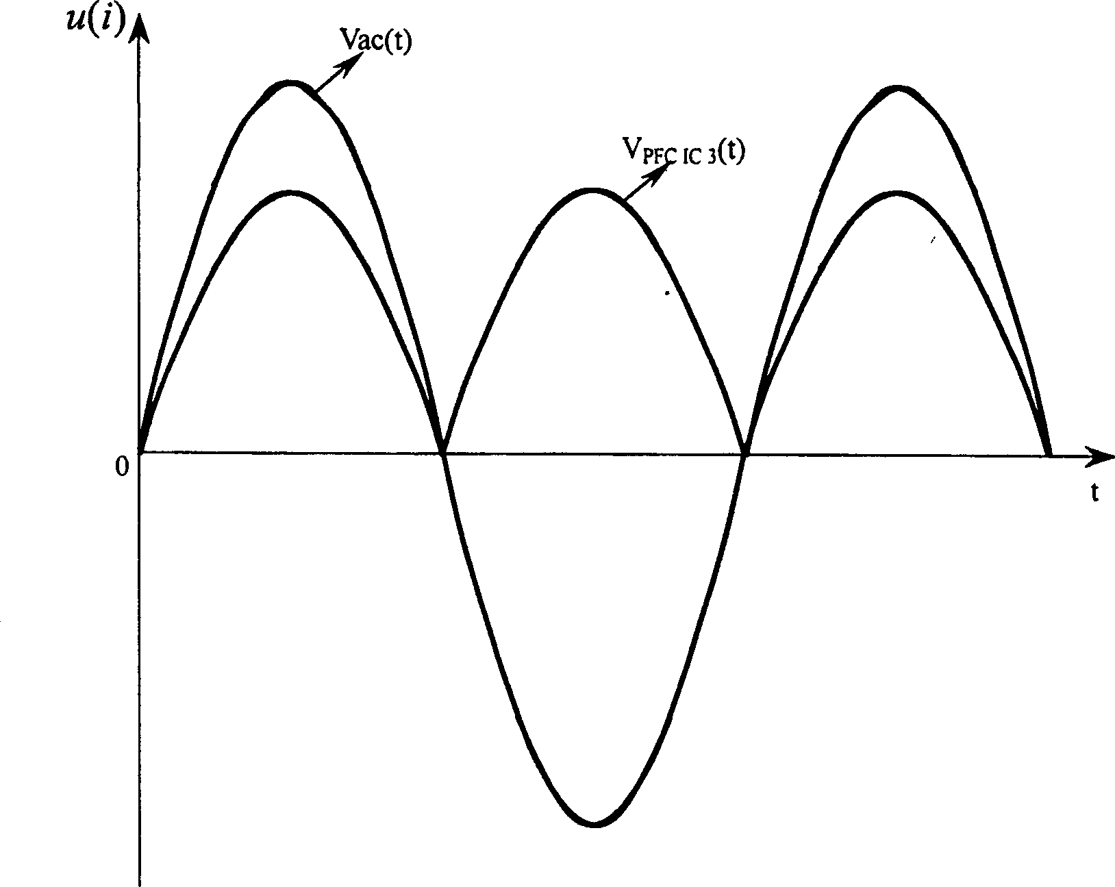
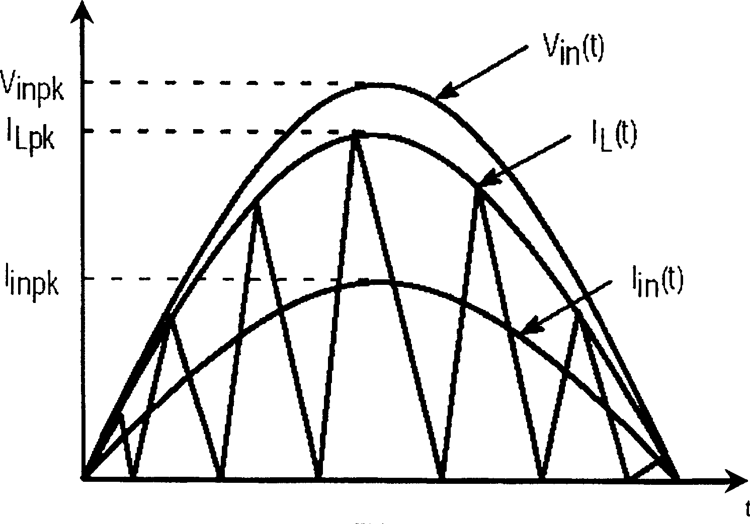
[0038] Because of the above reasons, the power factor correction circuit in the prior art appears such as Figure 4a , 4b 、Phenomenon 4c, that is, the zero-crossing distortion of the input current will increase with the increase of the power supply voltage

Method used


Image

  • Power factor correction circuit within broad voltage range
  • Power factor correction circuit within broad voltage range
  • Power factor correction circuit within broad voltage range

Examples


Embodiment 1

[0065] Embodiment 1: see Figure 7a , the transistor in the nonlinear compensation circuit is a crystal diode D1. The first voltage-dividing resistor R1 and the second voltage-dividing resistor R2 are connected in series to the output terminals of the rectifier circuit, that is, the input terminals A and B of the circuit, that is, one end of the first voltage-dividing resistor R1 is connected to the circuit input terminal A and connected to the third voltage-dividing resistor The piezoresistor R3 is connected to the common end of the primary coil of the boost inductor T1, the other end of the first voltage dividing resistor R1 is connected to the second voltage dividing resistor R2 and one end of the filter capacitor C1, and the other end of the second voltage dividing resistor R2 The other end of the filter capacitor C1 is connected to the circuit input terminal B; the cathode of the regulator tube ZD1 is connected to the common point of the first voltage dividing resistor R1...

Embodiment 2

[0069] Example 2: see Figure 7b , the transistor in the nonlinear compensation circuit is a transistor TR1. The first voltage-dividing resistor R1 and the second voltage-dividing resistor R2 are connected in series to the output terminals of the rectifier circuit, that is, the input terminals A and B of the circuit, that is, one end of the first voltage-dividing resistor R1 is connected to the circuit input terminal A and connected to the third voltage-dividing resistor The piezoresistor R3 is connected to the common end of the primary coil of the boost inductor T1, the other end of the first voltage dividing resistor R1 is connected to the second voltage dividing resistor R2 and one end of the filter capacitor C1, and the other end of the second voltage dividing resistor R2 It is connected to the other end of the filter capacitor C1 and then connected to the circuit input terminal B; the cathode of the regulator tube ZD1 is connected to the common point of the first voltage ...


PUM


Abstract

A power factor correcting circuit within wide voltage range is composed of a boost up circuit consisting of boost inductor, diode, energy-accumulating capacitor and FET, a control circuit comprising power factor corrector chip and its peripheral elements, and an additional non-linear conpensating circuit for providing the compensation voltage to said control circuit and composed of two voltage-dividing resistors, filter capacitor, voltage-stabilizing diode and a transistor. Its advantage is basically no cross-zero distortion of input current.

Description

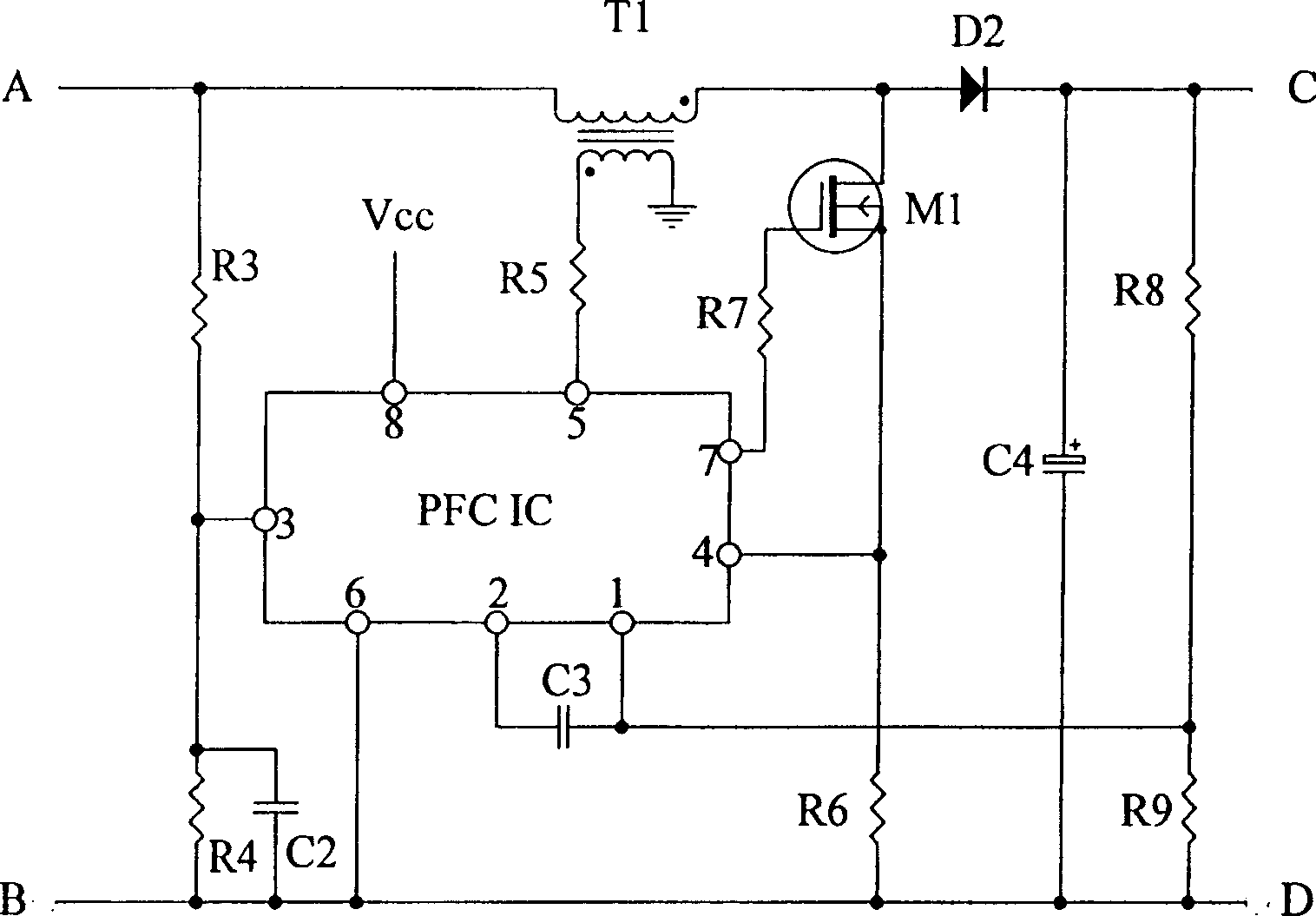
technical field [0001] The invention relates to a power factor correction circuit in power electronics, in particular to a power factor correction circuit within a wide voltage range. Background technique [0002] In the prior art, for low-power applications such as electronic ballasts, the power factor correction generally adopts critical conduction mode technology, such as figure 1 shown. The circuit mainly includes two parts: Boost Boost circuit and control circuit. The boost circuit is composed of the primary coil of the boost inductor T1, the freewheeling diode D2, the field effect transistor M1 and the energy storage capacitor C4; the control circuit is mainly composed of a power factor correction integrated chip working in the critical conduction mode peak current detection state PFC IC and its peripheral components. [0003] refer to figure 1 As shown, the signal of the input pin 3 of the internal multiplier of the power factor correction integrated chip PFC IC i...

Claims


Application Information

Patent Timeline
Patent Type & Authority Patents(China)
IPC IPC(8): H02M1/00H05B41/14G05F1/70H02M1/42
CPCY02B70/126Y02B70/10Y02P80/10
Inventor 曾浩然程玮
Owner FEIHONG ELECTRONICS SUZHOU
Learn More