Liquid crystal display device and driving method and circuitry thereof

A technology of liquid crystal display and driving method, which is applied to static indicators, instruments, circuits, etc., and can solve problems such as abnormality, which must be rebooted before restarting, and instant booting cannot be achieved.

Inactive Publication Date: 2007-03-07
HANNSTAR DISPLAY CORPORATION
View PDF3 Cites 0 Cited by
  • Summary
  • Abstract
  • Description
  • Claims
  • Application Information

AI Technical Summary

Problems solved by technology

And on the other hand, even if the switch from slant to bend is complete at the beginning of operation, in the subsequent operation, the liquid crystal cell in the optically compensated bend mode may cause the liquid crystal molecules to return to normal due to some specific reasons. To the state of slanting, at this time, the liquid crystal display will be abnormal, and the liquid crystal molecules that have been transferred to the state of slanting can ...

Method used


Image

  • Liquid crystal display device and driving method and circuitry thereof
  • Liquid crystal display device and driving method and circuitry thereof
  • Liquid crystal display device and driving method and circuitry thereof

Examples


Embodiment 1

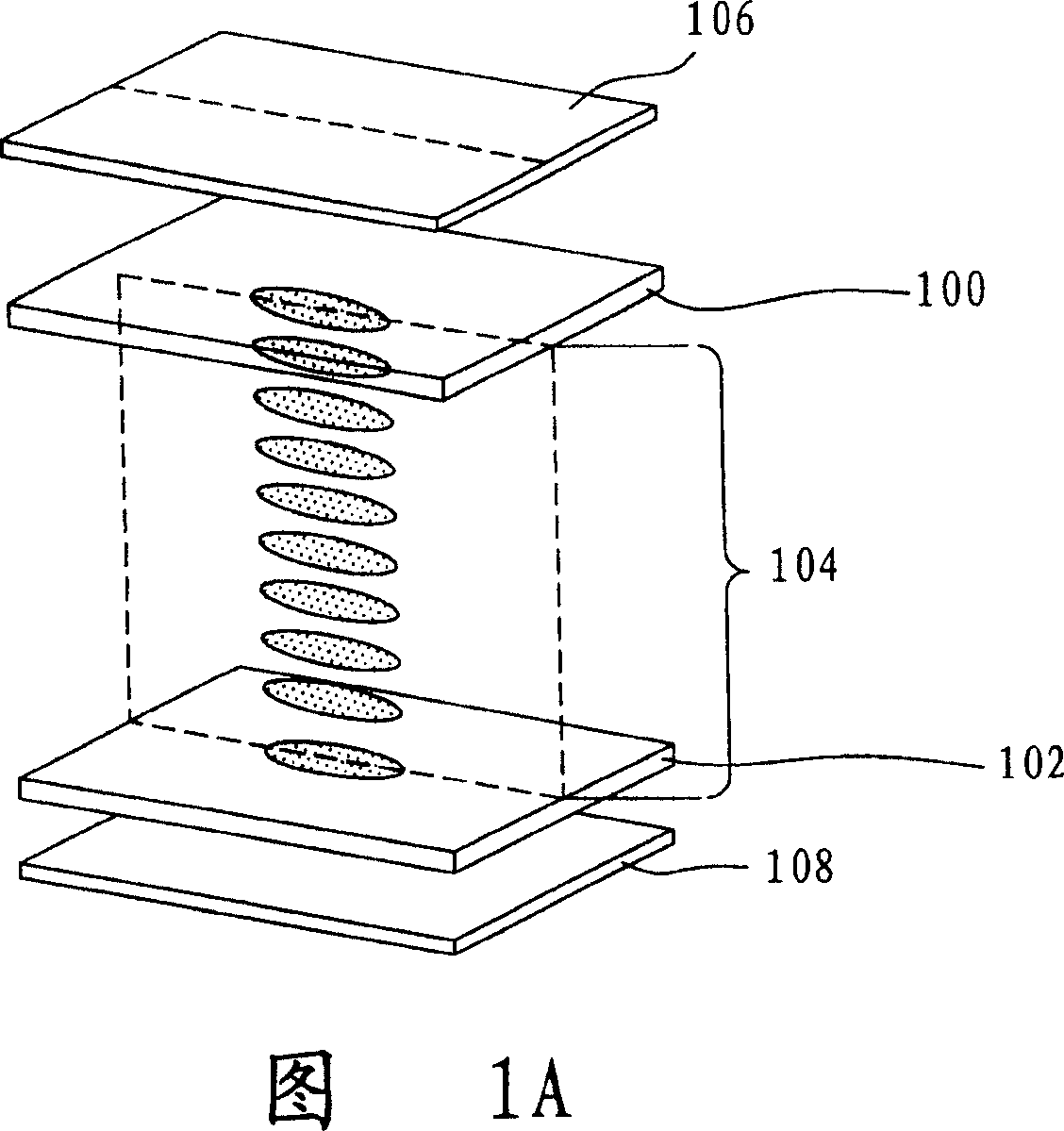
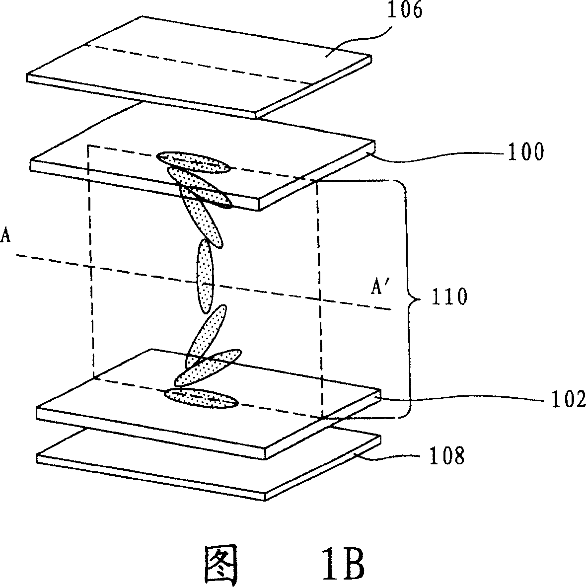
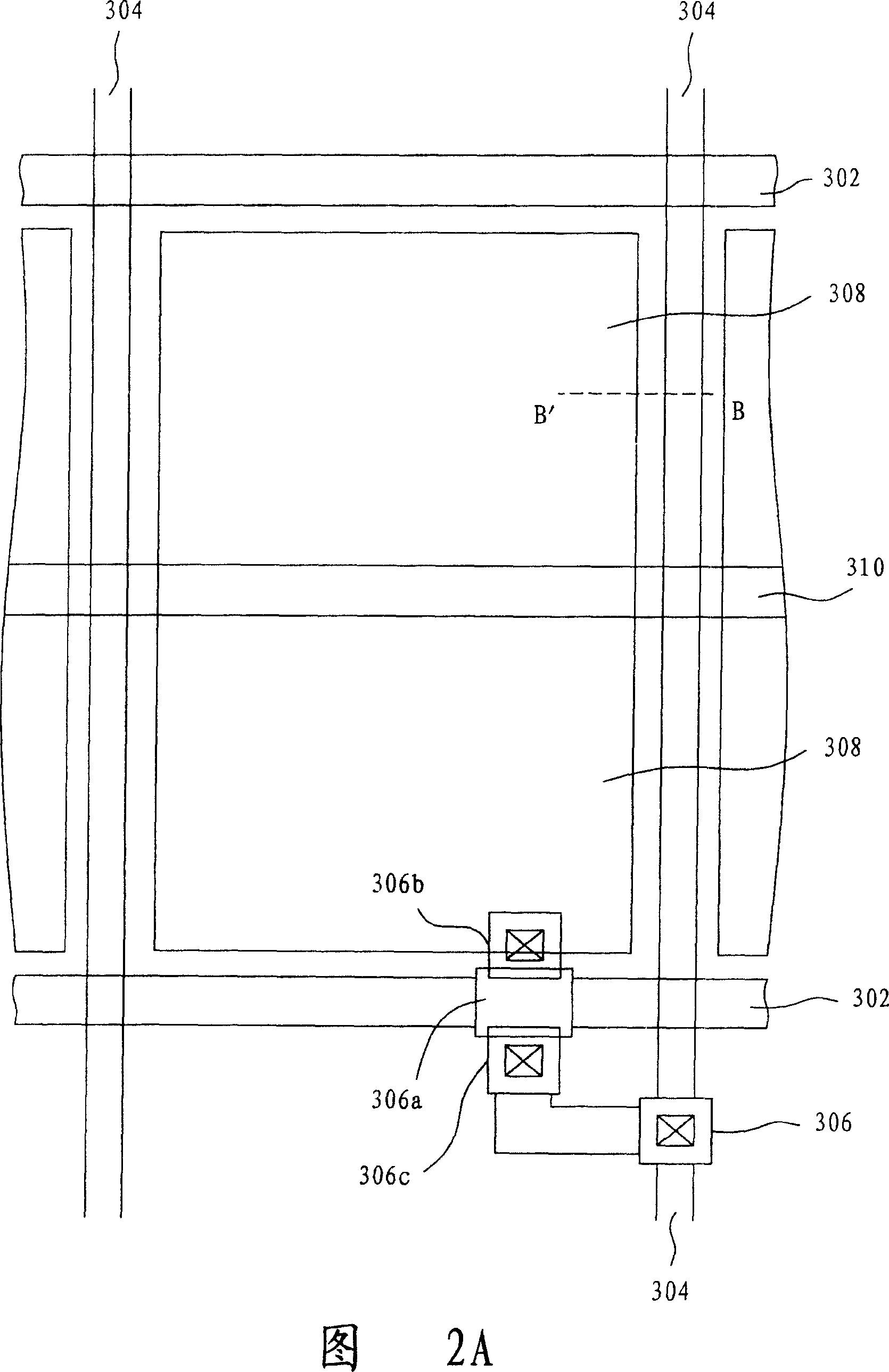
[0071] 3A is a top view of the pixel region of the first embodiment of the present invention, wherein the silicon island (silicon island) 506a of the switching transistor 506 is connected to the scanning line 502. When the switching transistor 506 is selected by the scanning signal, the scanning The signal will turn on the switching transistor 506, so the image signal on the image data line 504 will be transmitted and connected through the switching transistor 506, and the drain 506b of the switching transistor 506 is connected to the pixel electrode 508, and the other source 506c is connected to the image The data line 504 and a common electrode line 510 serve as the common electrode of the pixel electrode 508 . In the present invention, a metal electrode 512 is additionally arranged around the pixel electrode area, and the metal electrode 512 is controlled by the common electrode line 510 .

[0072] Generally speaking, for the pixel structure shown in FIG. 3A , for a selected...

Embodiment 2

[0078] 4A is a top view of the pixel region of the second embodiment of the present invention, wherein the silicon island (silicon island) 706a of the switching transistor 706 is connected to the scanning line 702. When the switching transistor 706 is selected by the scanning signal, the scanning The signal will turn on the switching transistor 706, so the image signal on the image data line 704 will be transmitted and connected through the switching transistor 706, and the drain 706b of the switching transistor 706 is connected to the pixel electrode 708, and the other source 706c is connected to the image The data line 704 and a common electrode line 710 are used as the common electrode of the pixel electrode 708. In the second embodiment of the present invention, a metal electrode 712 is arranged around the pixel electrode, and the metal electrode 712 is formed by the common electrode Controlled by line 710.

[0079] Please refer to FIG. 4B , which is a side view of the pix...

Embodiment 3

[0084] 5A is a top view of the pixel region according to the third embodiment of the present invention, wherein the silicon island (silicon island) 806a of the switching transistor 806 is connected to the scan line 802, and the drain 806b of the switching transistor 806 is connected to the pixel electrode 808. Another source electrode 806c is connected to the image data line 804, and a common electrode line 810 is used as the common electrode of the pixel electrode 808. In the third embodiment of the present invention, the metal electrode 812 and the common electrode 810 are in an "H" shape, And the metal electrode 812 is controlled by the common electrode line 810 .

[0085] Please refer to FIG. 5B , which is a side view of the pixel electrode according to the third embodiment of the present invention, which is a schematic cross-sectional view of the structure along line AA' in FIG. 5A . A lower substrate 814 and an upper substrate 816 formed of a transparent insulating mater...


PUM


Abstract

The LCD of the present invention has one additional electrode in the pixels, and the additional electrode is controlled with the common electrode. During LCD operation, one electric field is first applied to the additional electrode to convert the near liquid crystal molecules from inclined stretching state into bending state, and electric field is then applied onto the pixel electrode to make all the liquid crystal molecules in the pixel electrode into bending state. These two kinds of electric field may be also applied onto the common electrode and the pixel electrode separately and simultaneously.

Description

technical field [0001] The invention relates to a liquid crystal display pixel electrode structure and a liquid crystal display driving method and circuit. Background technique [0002] Twisted nematic cells (twisted nematic cells, TN cells) are currently widely used in color thin film transistor liquid crystal display (thin film transistor liquid crystal display, TFT LCD) components. However, the TFT liquid crystal display formed by the traditional twisted nematic liquid crystal cell has a very small viewing angle, so when viewing the liquid crystal display at an oblique angle, the contrast of the viewed screen is often reduced, and even the viewing angle is reduced. The image is reversed. Therefore, in order to solve the problem of narrow viewing angles, several methods have been proposed to manufacture screens with wide viewing angles. One of them is an alignment discrimination method, forming two or more alignment layers with different directions on each pixel electrod...

Claims


Application Information

Patent Timeline
IPC IPC(8): G02F1/136G02F1/1337G02F1/133H01L29/00
Inventor 吴昭慧杨界雄施博盛
Owner HANNSTAR DISPLAY CORPORATION
Why Eureka
Try Eureka