Preparation method of silicon carbide single crystal with low microtube density and silicon carbide single crystal

A technology of density silicon carbide and silicon carbide, applied in the field of silicon carbide crystal preparation, can solve problems affecting crystal quality, damaging the yield and reliability of semiconductor devices, and achieving the effect of low micropipe density

Pending Publication Date: 2021-09-28
ZHEJIANG UNIV HANGZHOU GLOBAL SCI & TECH INNOVATION CENT
View PDF10 Cites 0 Cited by
  • Summary
  • Abstract
  • Description
  • Claims
  • Application Information

AI Technical Summary

Problems solved by technology

[0004] Although many great advances have been made in the preparation of silicon carbide single crystals, there are some structural defects in the silicon carbide single crystal materials produced by conventional processes, especially the g

Method used


Image

  • Preparation method of silicon carbide single crystal with low microtube density and silicon carbide single crystal

Examples


Embodiment Construction

[0023] In order to facilitate the understanding of those skilled in the art, the present invention will be further described in detail below in conjunction with specific embodiments.

[0024] Embodiments of the present invention firstly provide a method for preparing a silicon carbide single crystal with low micropipe density.

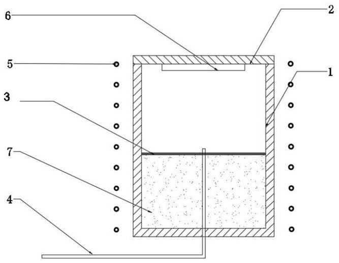
[0025] Please refer to figure 1 , is a cross-sectional view of a silicon carbide single crystal device with a low micropipe density prepared by using a method for preparing a silicon carbide single crystal with a low micropipe density according to an embodiment of the present invention.

[0026] In step 1, first put the crucible containing silicon carbide powder and assembled silicon carbide seed crystal into the crystal growth furnace and evacuate and depressurize the furnace. Inject protective gas to adjust the pressure and raise the temperature at the same time.

[0027] like figure 1 As shown, before forming the thermal gradient, a certain amoun...


PUM


Abstract

The invention provides a preparation method of a silicon carbide single crystal with low microtube density and the silicon carbide single crystal, and relates to the technical field of silicon carbide crystal preparation, the pressure in a furnace is increased from a first target pressure to a second target pressure by adjusting the flow rate of a protective gas, so that under the growth conditions of a first target temperature and the second target pressure, a thermodynamic equilibrium state is formed at a silicon carbide solid-gas interface, the surface of the silicon carbide single crystal originally provided with the microtube is reconstructed, and the silicon carbide single crystal subsequently generated on the surface of the silicon carbide single crystal has the advantages of low defect and low microtube density.

Description

technical field [0001] The invention relates to the field of silicon carbide crystal preparation, in particular to a method for preparing a silicon carbide single crystal with low micropipe density and the silicon carbide single crystal. Background technique [0002] As a third-generation wide-bandgap semiconductor material, silicon carbide has properties such as wide bandgap, high thermal conductivity, high electron saturation migration rate, and high breakdown electric field. It is considered ideal for manufacturing optoelectronic devices, high-frequency high-power devices, and high-temperature electronic devices. Semiconductor materials are widely used in white light lighting, optical storage, screen display, aerospace, oil exploration, automation, radar and communication, and automotive electronics. [0003] In the silicon carbide crystal growth method, the seed crystal and the silicon carbide source are set in the crucible, and then the crucible is heated to the sublima...

Claims


Application Information

Patent Timeline
IPC IPC(8): C30B29/36C30B23/00
CPCC30B29/36C30B23/00
Inventor 王亚哲皮孝东徐所成陈鹏磊姚秋鹏程周鹏罗昊
Owner ZHEJIANG UNIV HANGZHOU GLOBAL SCI & TECH INNOVATION CENT
Why Eureka
Try Eureka