Semiconductor package device with layer-increasing structure and making method thereof

A layer-building structure and packaging technology, which is applied in the manufacture of semiconductor/solid-state devices, semiconductor devices, semiconductor/solid-state device parts, etc., can solve the problems of inability to improve the reliability of finished products, chip 70 cracks, colloidal warping, etc. Problems, to achieve the effect of perfect protection, avoid gas explosion, not easy to absorb moisture

Active Publication Date: 2007-05-16
SILICONWARE PRECISION IND CO LTD
View PDF5 Cites 1 Cited by
  • Summary
  • Abstract
  • Description
  • Claims
  • Application Information

AI Technical Summary

Problems solved by technology

[0008] The U.S. Patent No. 6,498,387 uses a glass plate 71 as the carrier of the chip 70. The hard property of the glass plate 71 can solve the problem of warping and cracking of the colloid in the No. 6,271,469 patent, and because the glass plate 71 and The CTE of the chip 70 is similar, so there is no delamination problem caused by the above-mentioned CTE difference; however, the chip 70 is completely covered by the epoxy resin layer 72, often due to the thermal expansion coefficient of the chip 70 and the epoxy resin layer 72 The difference (CTE Mismatch) in the temperature cycle of the subsequent process will cause the chip 70 to be affected by the thermal stress and crack
At the same time, the side 720 of the epoxy resin layer 72 is directly exposed to the atmosphere, that is, due to the high hygroscopicity of the epoxy resin itself, the external moisture will accumulate on the active surface of the chip 70 through the epoxy resin layer 72, so It will cause the problem of popcorn, which will further prevent the reliability of the finished product from being improved

Method used


Image

  • Semiconductor package device with layer-increasing structure and making method thereof
  • Semiconductor package device with layer-increasing structure and making method thereof
  • Semiconductor package device with layer-increasing structure and making method thereof

Examples


Embodiment 1

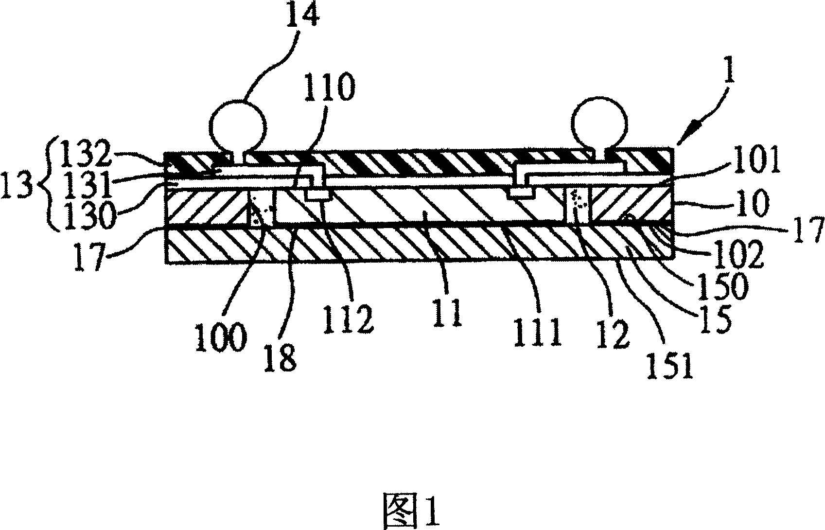
[0029]As shown in FIG. 1 , the wafer-level semiconductor package 1 with a build-up structure of the present invention mainly consists of a hard base 15, a hard frame 10 with a through hole 100, and is accommodated in the through hole 100 of the hard frame 10. The chip 11, the resin material 12 filled between the rigid frame 10 and the chip 11, the build-up structure 13 formed on the rigid frame 10 and the chip 11, and a plurality of solders implanted on the build-up structure 13 The ball (ie, the above-mentioned conductive component) 14 constitutes.

[0030] The hard base 15 and the hard frame 10 are made of glass material, metal material (such as copper metal, etc.), thermosetting material (such as polyimide resin (Polyimide Resin), BT resin (BismaleimideTriazine Resin) and FR-4, etc.) material, the hard base 15 and the hard frame 10 will not be warped and deformed under high temperature environment or temperature cycle in the manufacturing process, so it is used as the prima...

Embodiment 2

[0045] The manufacturing method to be disclosed in Embodiment 2 of the present invention is substantially the same as that in Embodiment 1 above, so only the differences will be described in detail with reference to the accompanying drawings, and the similarities will not be described again. In FIGS. 3A to 3B , the same or similar components as those in FIGS. 2A to 2F are denoted by the same reference numerals.

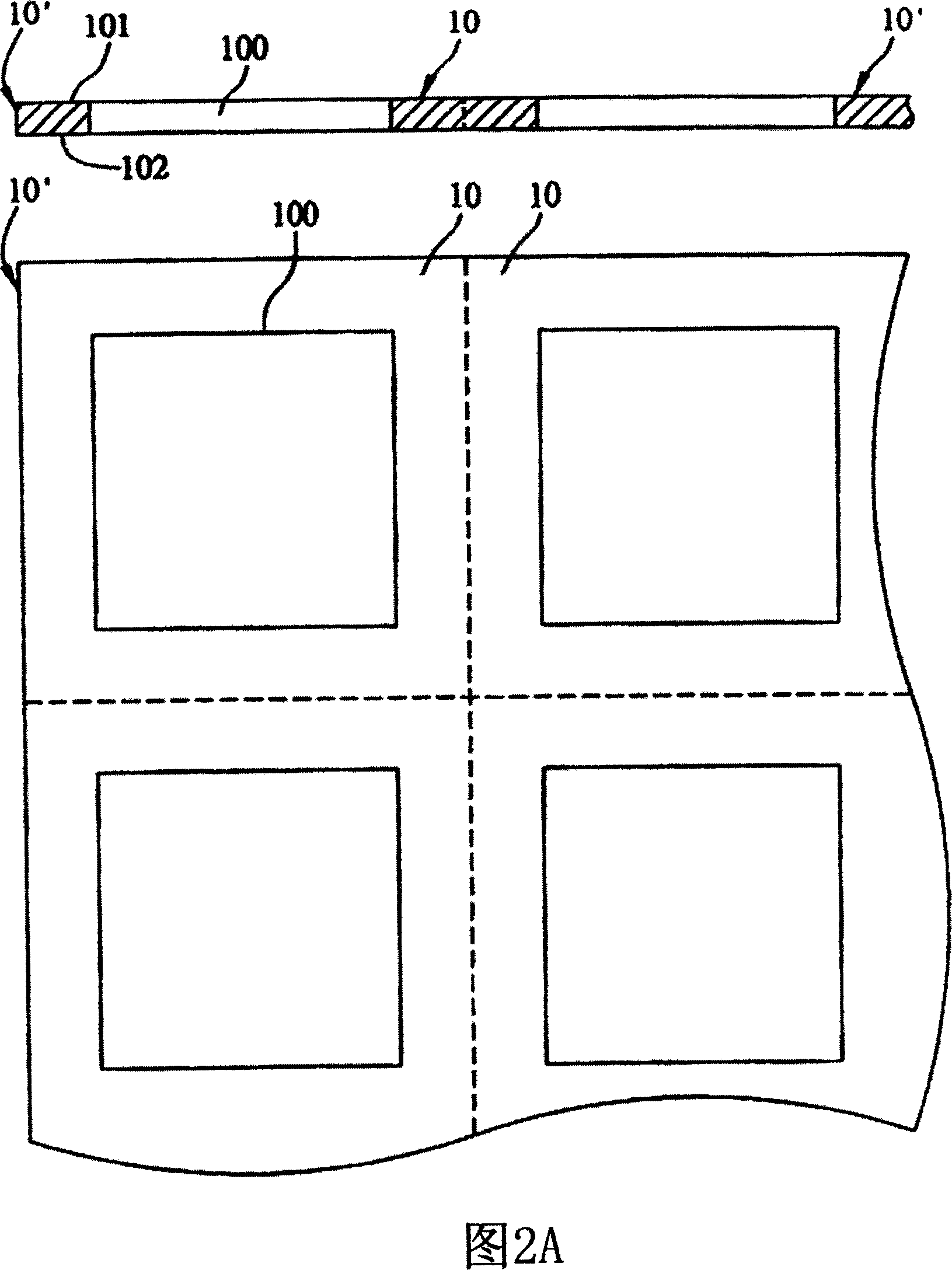
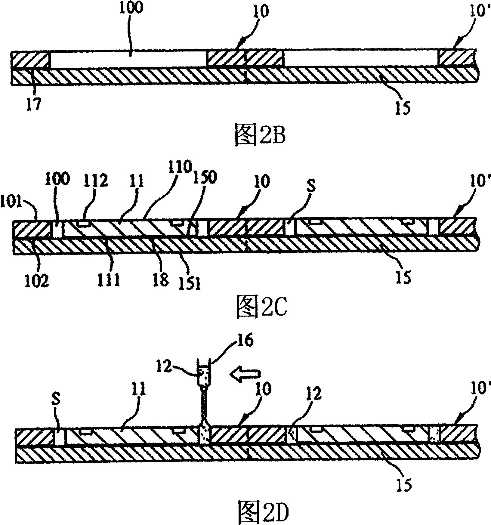
[0046] Referring to Fig. 3A, prepare the module board 10 ' that is made of a plurality of hard frames 10 that are arranged in an array, each hard frame 10 has a rectangular through hole 100, a first surface 101 and an opposite second surface 102; meanwhile, prepare The hard base 15 has a first surface 150 and a second surface 151 , and a plurality of chips 21 are fixed at predetermined positions on the hard base 15 . The fixing method is to apply bonding glue 18 on at least one surface of the first surface 150 of the hard base 15 and the non-active surface 111 of the ...

Embodiment 3

[0051]The structure of the wafer-level semiconductor package 4 to be disclosed in Embodiment 3 of the present invention is roughly the same as in Embodiment 1. The difference is shown in FIG. .

[0052] The manufacturing method of the semiconductor package 4 is to prepare a hard base 25, the hard base 25 has a first surface 250, a second surface 251 and at least one through hole 252, and the opening position of each of the through holes is in each corresponding The center of the chip preset position. Next, as in the first embodiment, the rigid frame 20 is fixed on the rigid base 25 with the adhesive material 27 . Then chip 21 is placed on the hard base 25, the chip 21 is placed in such a way that the non-active surface 211 of the chip 21 faces down to the through hole 252 of the hard base 25, and the gap between the chip 21 and the hard frame 20 A gap S is formed. After the chips 21 are loaded on the hard base 25 , the air is sucked out through the through holes 252 , so th...


PUM


Abstract

The capsulation piece comprises following parts: hard base, hard frame possessing through hole fixed on the hard base, at least one chip accommodated in the through hole of hard frame, medium filled in gap between chip and hard frame, addition layer structure formed on the chip and hard frame and connected to the chip electrically, multiple pieces of conducting subassemblies soldered on addition layer in use for connecting the chip to external devices electrically. Since the hard base and hard frame are adopted, the disclosed capsulation piece can prevent problems of structural warp, fragmentation, delamination and gas explosion etc. from happening. The invention discloses method for preparing the capsulation piece of semiconductor in wafer level further.

Description

technical field [0001] The present invention relates to a wafer-level semiconductor package and its manufacturing method, in particular to a build-up structure formed on the Active Surface of the chip, so that the exposed contacts (External Contacts) for solder ball implantation A wafer-level semiconductor package extending out of the active surface of the chip and its manufacturing method. Background technique [0002] In order to meet the requirements of thin, light and small electronic products, semiconductor packages, which are the core components of electronic products, are also developing in the direction of miniaturization. One form of miniaturized semiconductor package developed in the industry is chip scale package (Chip Scale Package, CSP), which is characterized in that the size of the chip scale package is equal to the size of the chip or about 1.2 larger than the size of the chip times. [0003] Furthermore, in addition to miniaturization in size, the semicond...

Claims


Application Information

Patent Timeline
Patent Type & Authority Patents(China)
IPC IPC(8): H01L23/02H01L23/48H01L21/60H01L21/50
CPCH01L24/97H01L24/19H01L2224/12105H01L2224/19H01L2224/32225H01L2224/32245H01L2224/73267H01L2224/92244H01L2924/181H01L2924/351H01L2924/00H01L2924/00012
Inventor 黄建屏萧承旭黄致明
Owner SILICONWARE PRECISION IND CO LTD
Why Eureka
Try Eureka