Array type optical probe scanning IC photoetching method

A technology for scanning integrated circuits and optical probes, applied in chemical instruments and methods, circuits, optics, etc., can solve problems such as difficulty in reducing and increasing production costs, and achieve the effect of simplifying the production process and high efficiency

Inactive Publication Date: 2002-01-30
TSINGHUA UNIV
View PDF0 Cites 6 Cited by
  • Summary
  • Abstract
  • Description
  • Claims
  • Application Information

AI Technical Summary

Problems solved by technology

[0009] First, due to the limitation of the numerical aperture of the lens and the wavelength of the light source, the minimum width of the circuit reticle has reached the limit, and it is difficult to continue to reduce it.
[0010] Second, this kind of projection scheme needs to make a set of masks every time a set of circuits is made, which will inevitably increase the production cost, especially for small batch production

Method used


Image

  • Array type optical probe scanning IC photoetching method
  • Array type optical probe scanning IC photoetching method
  • Array type optical probe scanning IC photoetching method

Examples


Embodiment Construction

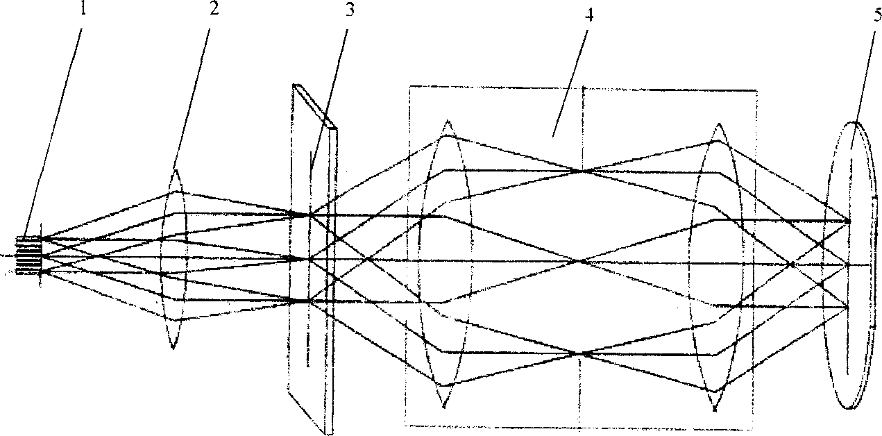
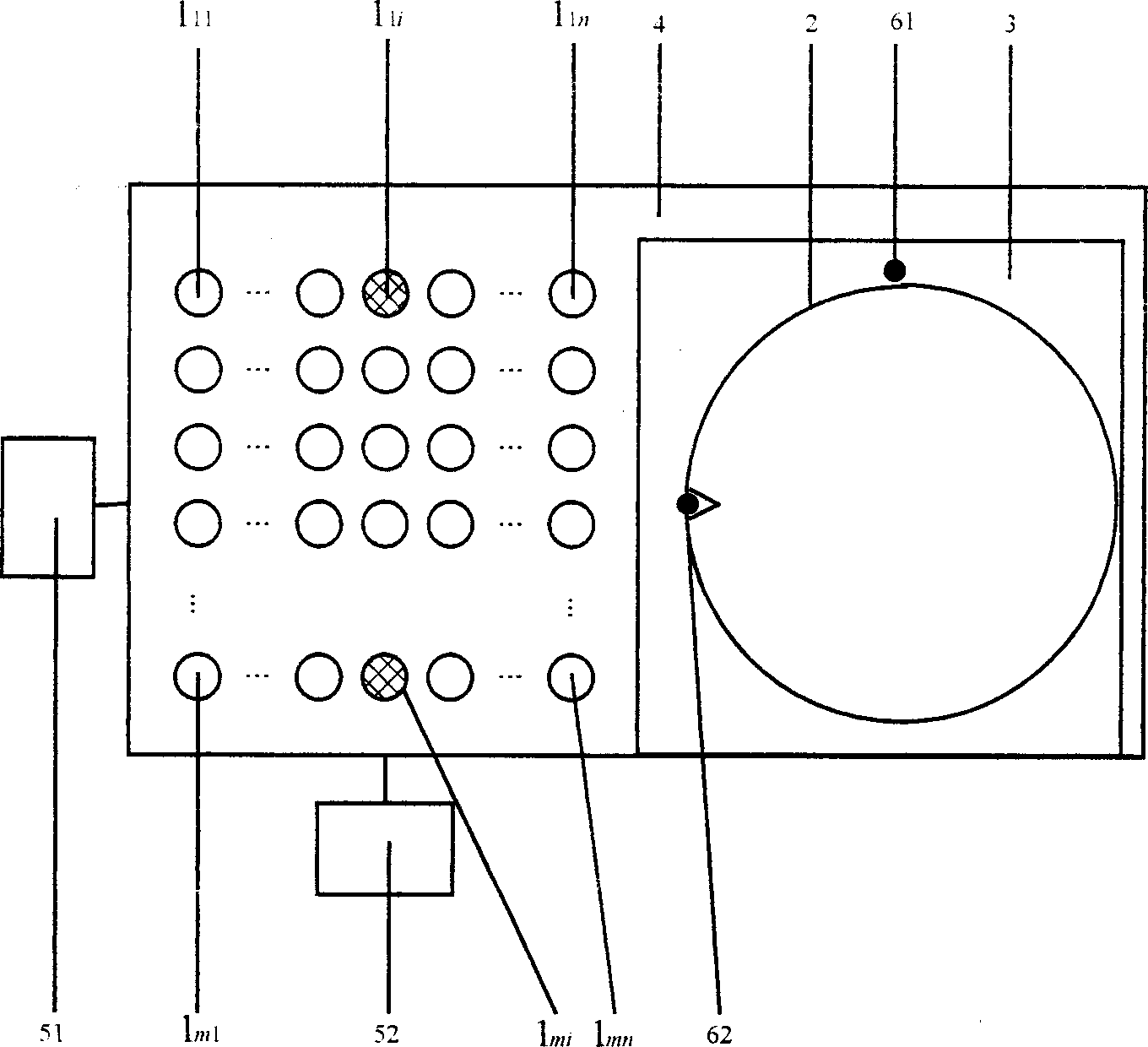
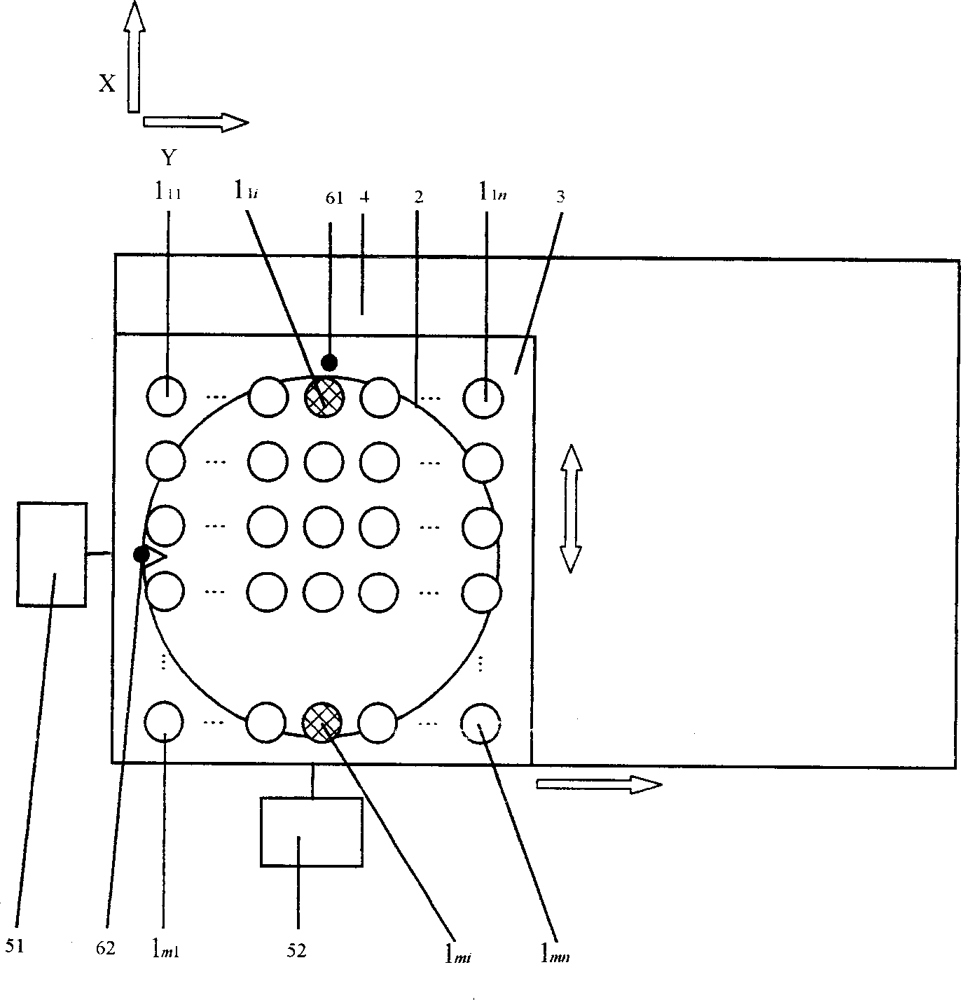
[0042] An embodiment of an array optical probe scanning integrated circuit lithography method proposed by the present invention is as follows figure 2 , 3 Shown, in conjunction with accompanying drawing, describe in detail as follows:

[0043] The optical probe array of this embodiment is a 40*40 square array formed by 1600 probe units, and its X-direction and Y-direction intervals can be adjusted by a computer. The adjustment range is 8mm-20mm, and the adjustment value is written according to the desired The size of the integrated circuit chip is determined. Probe unit 1 at the upper and lower ends li and 1 mi A unit for precise alignment in an array, with both read and write capabilities. When writing the circuit pattern, the movement and switching state of other units are the same. When performing precise alignment, they can read the signal on the silicon wafer, ensuring that the same silicon wafer is in a matching position every time it is written. whole unit 1 il ...


PUM


Abstract

The present invention belongs to the field of microfine engineering manufacture technology, and is characterizedb by that a kind of array optical probe scanning photoetching process is used to make integrated circuit so as to can make mininum wire width of integrated circuit less than 0.1 micrometer, at the same time it features quick speed and high efficiency. It can greatly simplify production process of integrated circuit, and provides a new effective pathway for making super-large-scale integrated circuit.

Description

technical field [0001] The invention belongs to the field of micro-engineering manufacturing, in particular to a method for manufacturing an integrated circuit by scanning an array type optical probe. Background technique [0002] The scale of integrated circuits is getting bigger and bigger, and the requirements for the line width of integrated circuits are getting smaller and smaller. At present, in the production of integrated circuits, the wavelength of incident light has been reduced to 260nm, the numerical aperture of the lens has reached 0.8, and the minimum line width of the circuit has reached 0.18μm, which is close to the physical limit. The existing manufacturing methods of integrated circuits are mainly optical projection manufacturing methods, such as figure 1 As shown, its production steps are as follows: [0003] 1) Make a set of different mask patterns 3; [0004] 2) Concentrating lens 2 gathers the light emitted by light source 1, and forms a correspondin...

Claims


Application Information

Patent Timeline
Patent Type & Authority Applications(China)
IPC IPC(8): B81C99/00G03F7/00H01L21/027
Inventor 徐端颐齐国生范晓冬李庆祥钱坤蒋培军
Owner TSINGHUA UNIV
Why Eureka
Try Eureka