

Conductive nitride film, process for producing the same, and antireflection object
A technology of nitride film and conductivity, applied in the direction of non-metallic conductors, conductive layers on insulating carriers, sputtering plating, etc., can solve problems such as pressure changes, prolonged vacuum exhaust time, and reduced conductivity
- Summary
- Abstract
- Description
- Claims
- Application Information
AI Technical Summary
Problems solved by technology
Method used
Image

Examples
Embodiment 1
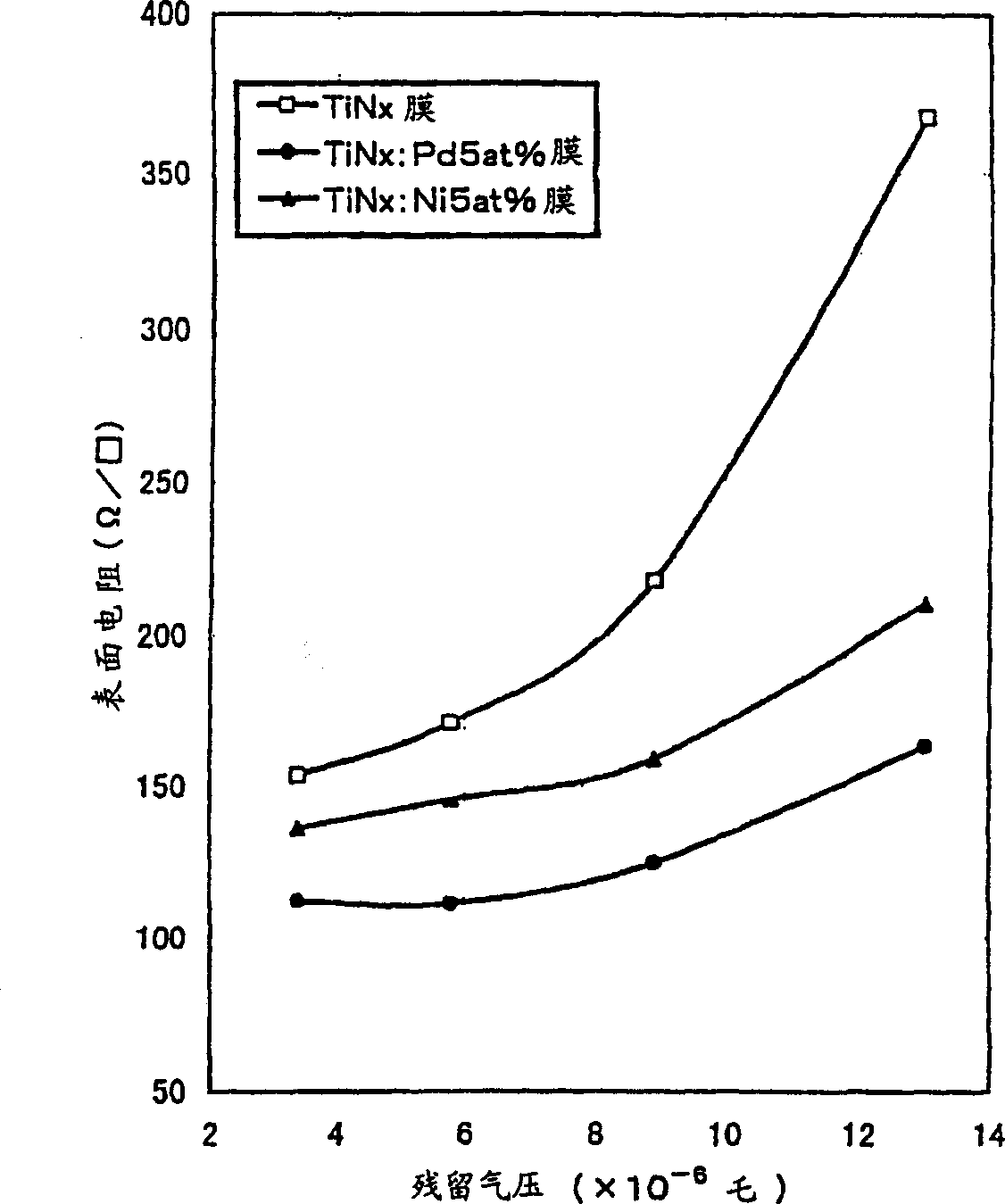
[0050] At a residual air pressure of 1.3 x 10 -5 Torr (1.73×10 -3 Pa) (approximately 5×10 -6 Torr (6.65×10 -4 Pa) is large, residual gas is large), Ar:N 2 =9:1 (volume ratio) mixed gas (6mm Torr (798mmPa)) atmosphere, at a power density of 2.2W / cm 2 Under the condition of , the Ti target containing Pd5at% (only Pd except Ti) is used to form a film on the glass substrate by the magnetron DC sputtering method. The obtained nitride film is a titanium nitride film (TiN x : Pd5at% film) with a film thickness of 20 nm.
[0051] The surface resistance (R s ), the difference in resistance between batches after 5 batches of film formation, and the change in resistance after heat resistance test (250°C, 30 minutes). The results are shown in Table 1.
Embodiment 2
[0053] Film formation was carried out in the same manner as in Example 1, except that the target used in Example 1 was replaced with a Ti target containing Ni 5 at % (only Ni in addition to Ti). The obtained nitride film is a titanium nitride film (TiN x : Ni5at% film), the film thickness is 20nm. The same measurement as in Example 1 was performed. The results are shown in Table 1.
Embodiment 3
[0055] A film was formed in the same manner as in Example 1 except that the target used in Example 1 was replaced with a Ti target. The obtained nitride film is titanium nitride film (TiN x film), the film thickness is 20nm. The same measurement as in Example 1 was performed. The results are shown in Table 1.
[0056] As can be seen from Table 1, with TiN x films compared to the inventive TiN x : Pd5at% film and TiN x : The difference in resistance between batches of Ni5at% film and the change in resistance after the heat resistance test are much smaller, and the repeatability and heat resistance are also very good.
[0057] Example
PUM
| Property | Measurement | Unit |
|---|---|---|
| Film thickness | aaaaa | aaaaa |
| Surface resistance | aaaaa | aaaaa |
| Surface resistance | aaaaa | aaaaa |
Abstract
Description
Claims
Application Information