Method of fabricating semiconductor device

A manufacturing method, semiconductor technology, applied in the direction of semiconductor/solid-state device manufacturing, semiconductor lasers, instruments, etc., can solve problems such as uneven composition, increased optical loss, and polluted surfaces, so as to achieve yield and quality improvement and avoid compositional inhomogeneity Effect

Inactive Publication Date: 2002-06-26
QINETIQ LTD
View PDF0 Cites 0 Cited by
  • Summary
  • Abstract
  • Description
  • Claims
  • Application Information

AI Technical Summary

Problems solved by technology

First, the entire process is complex and time-consuming
Second, removal of the partially grown wafer from the growth apparatus and etching of the waveguide core can contaminate the waveguide, increasing optical loss and reducing yield
Third, the reproducibility of these methods is very low
This technique includes additional growth steps for dielectric aperture growth and additional processing steps to remove the dielectric aperture, as well as processing for patterning the aperture, which introduces significant delays and can contaminate the surface
Although mechan...

Method used


Image

  • Method of fabricating semiconductor device
  • Method of fabricating semiconductor device
  • Method of fabricating semiconductor device

Examples


Embodiment Construction

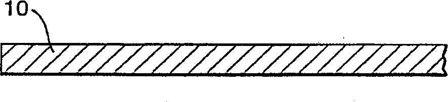
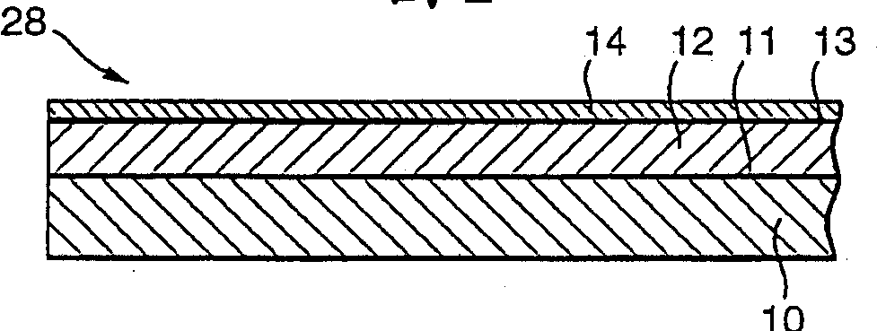
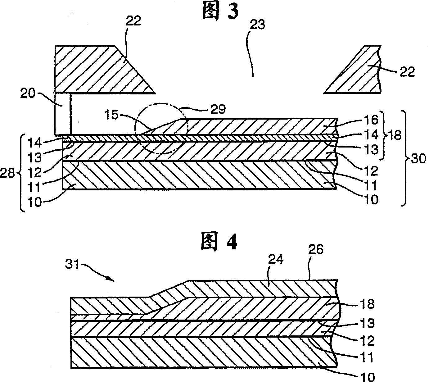
[0030] refer to figure 1 , a portion of a vertical cross-section of a gallium arsenide (GaAs) based wafer 10 is shown in the figure. Substrate 10 has been prepared for epitaxial growth according to standard procedures well known to those skilled in the art of semiconductor device fabrication. The substrate 10 is mounted on a molybdenum holder (not shown). The mounted substrate 10 is placed in a chemical beam epitaxy (CBE) apparatus, and then stored under ultra-high vacuum (UHV). Then put the substrate 10 into the growth chamber of the CBE device under ultra-high vacuum, and heat it to about 650 degrees Celsius under the ultra-high pressure of arsenide to remove the oxide deposition on the surface, while maintaining a stable surface and avoiding It gets rough. The temperature of substrate 10 is then set to a growth temperature in the range of 400 to 700 degrees Celsius, typically 540 degrees Celsius, to reduce unintentional accumulation of impurities during CBE growth using ...


PUM


Abstract

A method of fabricating a semiconductor device includes a step of growing at least one tapered epitaxial layer upon a supporting surface by chemical beam epitaxy, the plane of the taper being inclined to the supporting surface.

Description

technical field [0001] The invention relates to a method for manufacturing a semiconductor device with a tapered epitaxial layer. Background technique [0002] Optoelectronic systems include optical fibers and optoelectronic semiconductor devices such as lasers, amplifiers, modulators, detectors, and switches. The size and shape of the optical modes supported by optical fibers are very different from those in opto-semiconductor devices, leading to mode mismatches and high optical loss. [0003] One technique that can reduce this optical loss is to place a microlens between the optoelectronic semiconductor device and the optical fiber. Microlenses can change the size of the optical mode output of an optoelectronic semiconductor device or optical fiber, but will not change the shape of the optical mode. Another technique is to place an optical mode conversion waveguide between the optoelectronic semiconductor device and the optical fiber. Both technologies require very hig...

Claims


Application Information

Patent Timeline
IPC IPC(8): G02B6/12G02B6/122G02B6/13H01L21/205
CPCH01S2304/10G02B6/1228G02B2006/12078G02B6/131
Inventor T·马丁R·S·巴尔默S·G·艾林J·O·麦克莱恩J·M·赫顿
Owner QINETIQ LTD
Why Eureka
Try Eureka