Surface mount package for power semiconductor devices
A technology for semiconductor tubes and main surfaces, applied in semiconductor devices, semiconductor/solid-state device parts, electric solid-state devices, etc., can solve problems such as die cracking
- Summary
- Abstract
- Description
- Claims
- Application Information
AI Technical Summary
Problems solved by technology
Method used
Image

Examples
Embodiment Construction
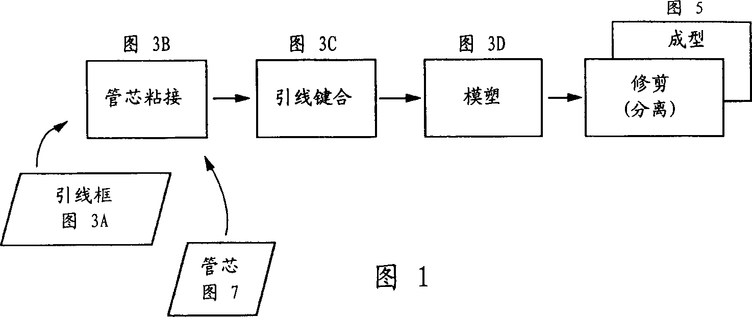
[0142] Figures 14A to 14I Structures are shown for various bond-wireless (BWL) packages for two-terminal devices such as PIN diodes, transient suppressors, Zener diodes, etc., which require surface mount packaging. This packaging technique can also be used for capacitors, fuses and other passive components.
[0143] exist Figure 14A In the structure of the package 300, two lead frames 302 and 304 are substantially parallel and sandwich a semiconductor die 306 having conductive upper and lower surfaces. Leadframes 302 and 304 are bonded to die 306 by intermediate layers 308 , 310 of conductive epoxy (silver filled) or solder. Leadframe wires protrude from package 300 at two different heights (relative to the circuit board) and are bent into coplanar wire tails 302A and 304A for mounting on surface 310 of the printed circuit board. Assembly involves mounting the die 306 onto the first lead frame 304, as shown in the plan view of FIG. 14B or the cross-sectional view of FIG. ...
PUM
 Abstract
Description
Claims
Application Information
 - R&D
- Intellectual Property
- Life Sciences
- Materials
- Tech Scout
- Unparalleled Data Quality
- Higher Quality Content
- 60% Fewer Hallucinations
Browse by: Latest US Patents, China's latest patents, Technical Efficacy Thesaurus, Application Domain, Technology Topic, Popular Technical Reports.
© 2025 PatSnap. All rights reserved.Legal|Privacy policy|Modern Slavery Act Transparency Statement|Sitemap|About US| Contact US: help@patsnap.com