Wire frame and the manufacture of resin sealed semiconductor unit with the wire frame

A manufacturing method and semiconductor technology, applied in semiconductor/solid-state device manufacturing, semiconductor devices, semiconductor/solid-state device components, etc., can solve problems such as mesh blockage, poor installation tightness of mounting substrates, and poor electrical connections

Inactive Publication Date: 2002-09-25
TESSERA ADVANCED TECH
View PDF0 Cites 5 Cited by
  • Summary
  • Abstract
  • Description
  • Claims
  • Application Information

AI Technical Summary

Problems solved by technology

[0005] Like this, if produce burr 101a on the bottom surface of semiconductor device 100, then when this semiconductor device 100 is the surface mount type that the bottom surface exposes lead wire, because the existence of burr 101a, make it and the mounting tightness between mounting substrate deteriorate, It is easy to cause the problem of poor electrical connection
[0006] Moreover, the cutting surface of the cutting blade 201 is usually coated with powder such as diamond, and when the lead frame 101 made of metal is repeatedly cut, there is also the following problem: that is, the cutting surface is prone to sieve due to the metal powder. clogged eye problem

Method used


Image

  • Wire frame and the manufacture of resin sealed semiconductor unit with the wire frame
  • Wire frame and the manufacture of resin sealed semiconductor unit with the wire frame
  • Wire frame and the manufacture of resin sealed semiconductor unit with the wire frame

Examples


Embodiment Construction

[0040] Hereinafter, embodiments of the present invention will be described in detail with reference to the drawings.

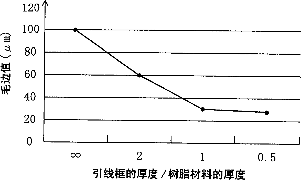
[0041] In a method of manufacturing a resin-sealed semiconductor device by cutting one lead frame of a plurality of semiconductor devices that are resin-sealed with a dicing member such as a dicing blade, while suppressing the occurrence of burrs due to the blade, in order to improve the As a result of many studies on the decrease in productivity due to clogging of blade meshes, the following findings were obtained.

[0042] figure 1 Indicates the relationship between the ratio of the thickness of the lead frame to the thickness of the sealing resin material and the value (height) of burrs generated during cutting. Here, using a lead frame made of copper (Cu) alloy and a cutting blade having a width of 0.1 mm to 0.9 mm, the lead frame to be cut has a width of 0.11 mm to 0.99 mm. As cutting conditions, set the conveying speed of the cutting blade at 10mm / s~1...


PUM


Abstract

A lead frame 10 includes: a plurality of chip loading parts 12 supported by the outer frame part 11 and respectively loading a plurality of semiconductor chips; inner lead parts 13 arranged around each chip loading part 12; The connecting portion 14 between the lead portion 13 and the outer frame portion 11 . The plurality of chip mounting portions 12 are surrounded by a sealing region 20 that is entirely sealed with a sealing resin. Outside the sealing area 20 of the outer frame portion 11 of the lead frame 10 and in the area on the extension line of the connecting portion 14, a first opening portion 16 having a width larger than that of the dicing blade is provided. To improve the quality of a resin-sealed semiconductor device by reducing burrs generated on the cut surface of a lead frame, while prolonging the life of a dicing blade and improving production efficiency.

Description

technical field [0001] The present invention relates to a lead frame in which the lead frame is exposed from the bottom surface after resin sealing, and a method of manufacturing a surface-mountable resin-sealed semiconductor device using the lead frame. Background technique [0002] In recent years, there has been an increasing demand for high-density packaging of semiconductor components in order to meet the miniaturization and higher functionality of electronic devices. Accompanying this demand, the miniaturization and thinning of resin-sealed semiconductor devices, in which semiconductor chips and leads are integrally packaged with molded resin materials, are rapidly progressing, and researchers are conducting various researches in order to reduce production costs and improve production efficiency. effort. [0003] Next, a conventional method of manufacturing a resin-sealed semiconductor device will be described with reference to the drawings. [0004] Figure 11 It sh...

Claims


Application Information

Patent Timeline
Patent Type & Authority Applications(China)
IPC IPC(8): H01L23/28H01L21/56H01L21/68H01L23/12H01L23/31H01L23/495H01L23/50
CPCH01L21/561H01L21/565H01L21/568H01L23/3107H01L23/49548H01L24/97H01L2224/48091H01L2224/48247H01L2224/97H01L2924/01029H01L2924/01033H01L2924/01082H01L24/48H01L2924/01005H01L2924/01006H01L2924/181H01L24/45H01L2224/05599H01L2224/451H01L2224/85399H01L2924/00014H01L2924/14H01L2224/85H01L2924/00012H01L2224/45015H01L2924/207H01L2924/00H01L23/28
Inventor 内海胜喜船越正司滨谷毅森川健中林幸男
Owner TESSERA ADVANCED TECH
Why Eureka
Try Eureka