Photoetching method for nanoparticle pattern based on self organization

A nano-lithography and nano-particle technology, applied in electrical components, semiconductor/solid-state device manufacturing, circuits, etc., can solve problems such as lack of versatility, and achieve good compatibility and simple process.

Inactive Publication Date: 2003-01-15
SHANGHAI HUA HONG GROUP +1
View PDF0 Cites 17 Cited by
  • Summary
  • Abstract
  • Description
  • Claims
  • Application Information

AI Technical Summary

Problems solved by technology

But this method is only applicable to specific substrates and quantum dot systems, and lacks generality

Method used


Image

  • Photoetching method for nanoparticle pattern based on self organization
  • Photoetching method for nanoparticle pattern based on self organization
  • Photoetching method for nanoparticle pattern based on self organization

Examples


Embodiment Construction

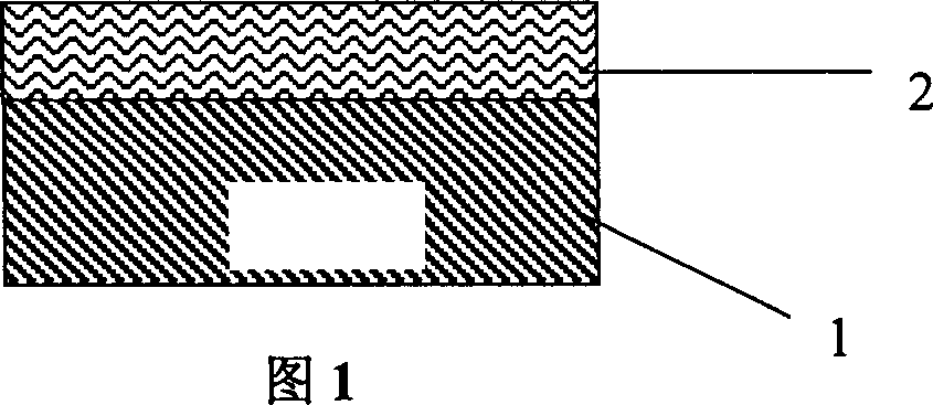
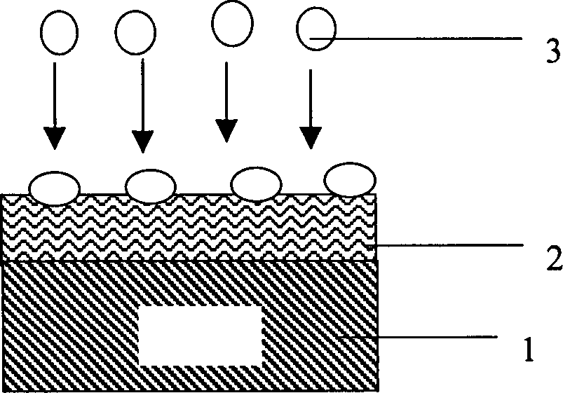
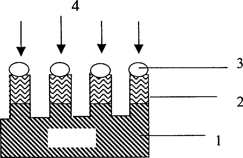
[0017] Taking the Si substrate material as an example (the basic process flow of other substrates such as Ge, GaAs, SOI, etc. is the same), the method is further described in detail. Its production process is as shown in Figure 1- Figure 4 Shown:

[0018] 1. Preparation of submicron periodic templates (Figure 1):

[0019] (1) Select an appropriate organic substance, such as polystyrene-polybutadiene or polydimethylsiloxane, as a template material.

[0020] (2) Form a periodic and ordered spatial self-organization structure on the surface of the substrate through the self-assembly of organic substance molecules or driven by the outside world (such as noise regulation). From the perspective of process compatibility, mainly through organic vapor deposition, high-speed spin coating (spincoating) and high-vacuum anion polymerization technology, combined with substrate induction, noise control and other methods, the formation of template materials such as block copolymers on the ...


PUM


Abstract

The ordered array and pattern of nanoparticles formed by gas-phase or liquid-phase deposition is used to replace the mask generated by exposure used in photoetch technology, resulting in structural size less than 10 nm. It features that the copolymer film is used as template to guide the assembling of nanoparticles. Its advantage is high versatility to different substrates.

Description

technical field [0001] The invention belongs to the technical field of integrated circuit manufacturing technology, and in particular relates to a new nanometer photolithography method. Background technique [0002] Traditional lithography techniques, such as light, electron beam, and ion beam exposure combined with dry or wet selective etching, have made the line width of devices thinner and thinner, and even surpassed many original so-called limits. However, as the line width further shrinks, lithography becomes more and more difficult, and the cost increases exponentially, which may encounter a real limit. On the other hand, with the recent rapid development of nanotechnology, new nanodevices will appear in the near future. Therefore, people are working hard to find new photolithography techniques to break through the traditional complex photolithography techniques to make nano-patterns. One of the techniques is to realize the fabrication of nanostructure arrays and dom...

Claims


Application Information

Patent Timeline
Patent Type & Authority Applications(China)
IPC IPC(8): C23F1/02H01L21/308H01L21/32H01L21/467H01L21/475
Inventor 韩民陈寿面
Owner SHANGHAI HUA HONG GROUP
Why Eureka
Try Eureka