Bottom buffering metal lug structure

A metal structure and buffer metal layer technology, which is applied to electrical components, electrical solid-state devices, circuits, etc., can solve the problems of weakening the bonding strength of the solder bump 18 and the bottom metal layer 100 of the bump, reducing the electrical performance of the chip 10, etc.

Inactive Publication Date: 2003-01-22
VIA TECH INC
View PDF0 Cites 28 Cited by
  • Summary
  • Abstract
  • Description
  • Claims
  • Application Information

AI Technical Summary

Problems solved by technology

It should be noted that the intermetallic compound will increase the electrical resistance (electrical resistance) between the solder bump 18 and the UBM layer 100, which will reduce the electrical performance of the chip 10 after flip-chip packaging, and at the same time weaken the The bonding strength between the solder bump 18 and the under bump metallurgy layer 100

Method used


Image

  • Bottom buffering metal lug structure
  • Bottom buffering metal lug structure
  • Bottom buffering metal lug structure

Examples


Embodiment Construction

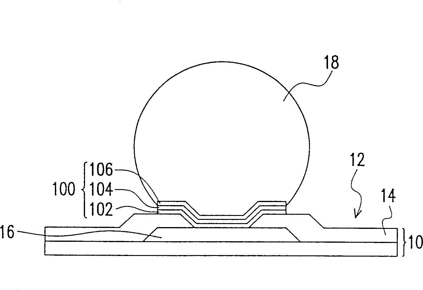
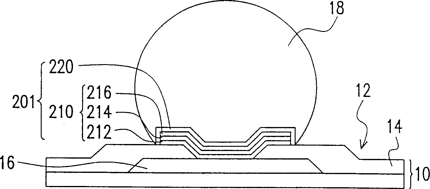
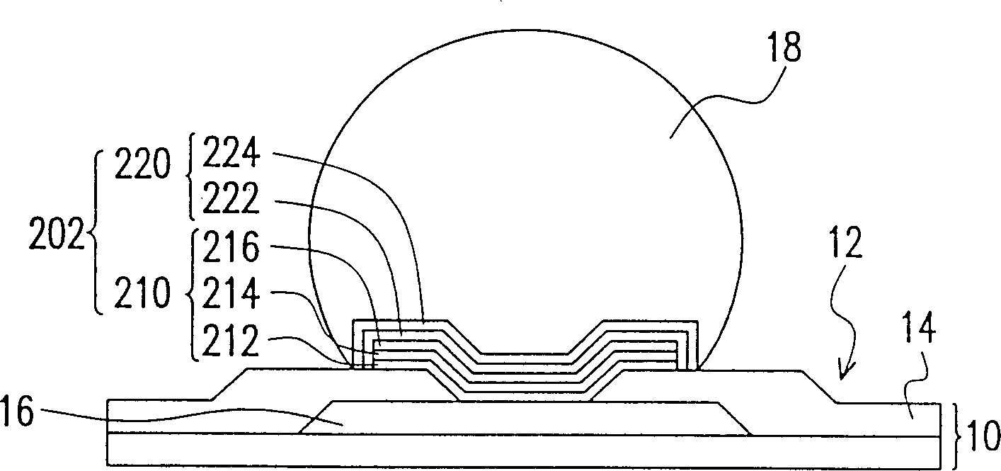
[0043] Please refer to Figure 2A , which is a schematic cross-sectional view of the first under-bump buffer metal structure according to a preferred embodiment of the present invention, which is disposed between a pad and a solder bump of a chip. The chip 10 has an active surface 12, a protection layer 14 and a plurality of pads 16 (only one of them is shown), and the protection layer 14 and the pads 16 are all configured on the active surface 12 of the chip 10, and the protection layer 14 is exposed The bonding pad 16 is above the active surface 12 of the chip 10 . It should be noted that the active surface 12 of the chip 10 generally refers to the side of the chip 10 with active components. In order to provide an interface for bonding between the solder pad 16 and the solder bump 18, the present invention proposes a first under-bump buffer metal structure 201 for disposing between the solder pad 16 and the solder bump 18, which mainly includes a metal layer 210 and a buffe...


PUM


Abstract

A bulge-bottom buffering metal structure is suitable for being disposed between a chip or a soldering pad for baseplate and a solder lug whose main component is tin-lead alloy. The said bulge-bottom buffering metal structure has at least one metal layer and one tuffing metal construction. This buffering metal construction can reduce or slow down the negative effect of electric and mechanical properties due to the generation of mesic metal compound when the metal layer combines with the solder lug. The metal layer disposed on the soldering pad of chip is composed of such components as Cu, Al, Ni, Ag or Au, etc. which may react on tin chemically, while the buffering construction disposed between the metal layer and the solder lug is used for reducing the possibility of generating the mesic metal compound between them.

Description

technical field [0001] The present invention relates to an under bump metal structure (Under Bump Metallurgy, UBM) that can be configured between a pad of a chip or a substrate and a solder bump, and in particular to a solder structure that can be configured on a chip or a substrate. Between the pad and the solder bump, the buffer metal structure under the bump is used to alleviate or slow down the generation of the inter-metallic compound (IMC). Background technique [0002] Flip Chip Interconnect Technology (Flip Chip Interconnect Technology) mainly uses the arrangement of area arrays to arrange multiple pads (pads) of a chip (die) on the active surface (active surface) of the chip. Form bumps on each pad, such as solder bumps, and then after flipping the chip, use the bumps on the pads of the chip to connect to the substrate or printed circuit board. (PCB) contacts on the surface. Since the flip-chip bonding technology is applicable to high pin count (High Pin Count) ch...

Claims


Application Information

Patent Timeline
Patent Type & Authority Applications(China)
IPC IPC(8): H01L21/28H01L21/60H01L21/768H01L23/48H01L23/52
CPCH01L24/03H01L24/05H01L2224/03849H01L2224/0401H01L2224/05556H01L2224/05557H01L2224/11H01L2224/11849H01L2224/13H01L2224/13019H01L2224/13082H01L2224/1354H01L2924/351
Inventor 宫振越何昆耀
Owner VIA TECH INC
Why Eureka
Try Eureka