Compound semiconductor device
A semiconductor and compound technology, applied in the field of compound semiconductor devices, can solve the problems of difficulty and failure in the use of silicon chips in high frequency bands
- Summary
- Abstract
- Description
- Claims
- Application Information
AI Technical Summary
Problems solved by technology
Method used
Image

Examples
Embodiment Construction
[0030] Refer to the following Figure 1 to Figure 4 Examples of the present invention will be described.
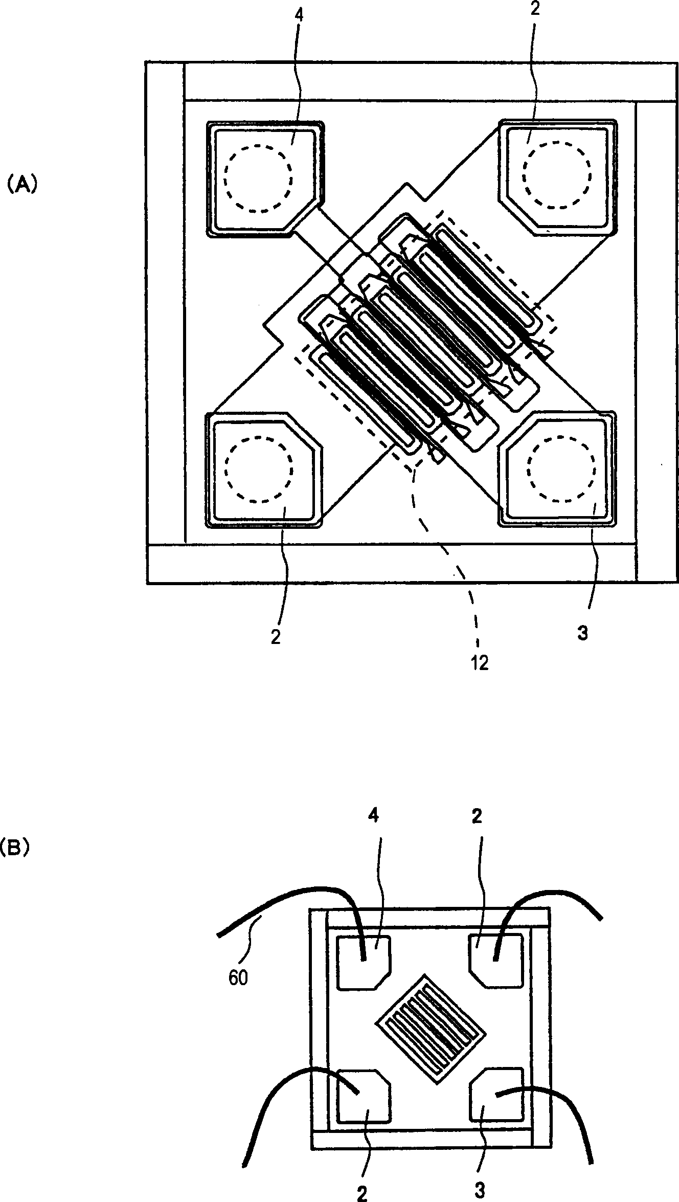
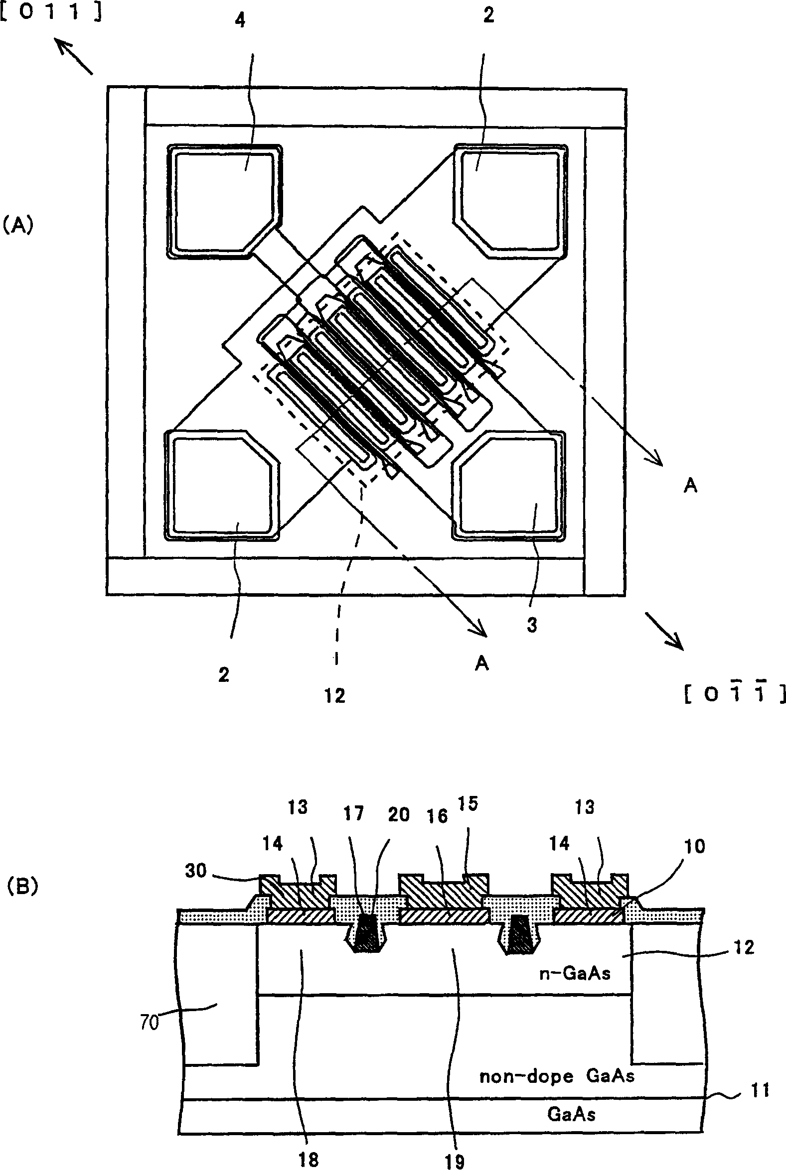
[0031] figure 1 (A) shows an example of a GaAsFET as the first embodiment of the present invention.
[0032]The GaAsFET is composed of a channel region 12 , a source contact electrode 2 , a drain contact electrode 3 , and a gate contact electrode 4 .
[0033] The channel region 12 is configured as follows. On the non-doped GaAs substrate, a non-doped buffer epitaxial growth layer and an N-type epitaxial growth layer are laminated, and a Schottky contact gate is arranged on the surface. Sources and drains in ohmic contact with the GaAs surface are arranged on both sides. The FET uses the gate potential to form a depletion layer in the channel region directly below, thereby controlling the drain current between the source and drain.
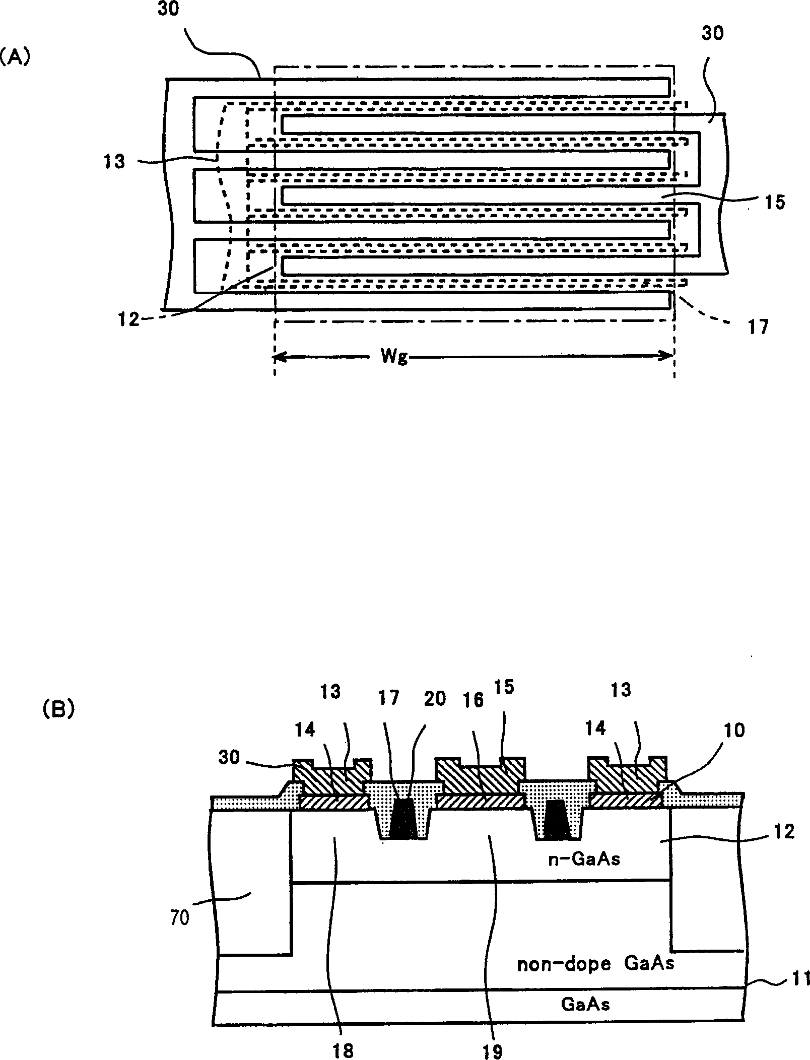
[0034] In this figure, a rectangular region surrounded by a dotted line is a channel region 12 formed in the substrate. The comb-shaped...
PUM
 Abstract
Description
Claims
Application Information