

Method for dipositing high-dielectric constant material on chip using atomic layer diposition method
A kind of atomic layer deposition and substrate technology, applied in metal material coating process, coating, circuit, etc., can solve the problems of occupying space, hindering single layer deposition, low dielectric constant, etc.
- Summary
- Abstract
- Description
- Claims
- Application Information
AI Technical Summary
Problems solved by technology
Method used
Image

Examples
Embodiment Construction
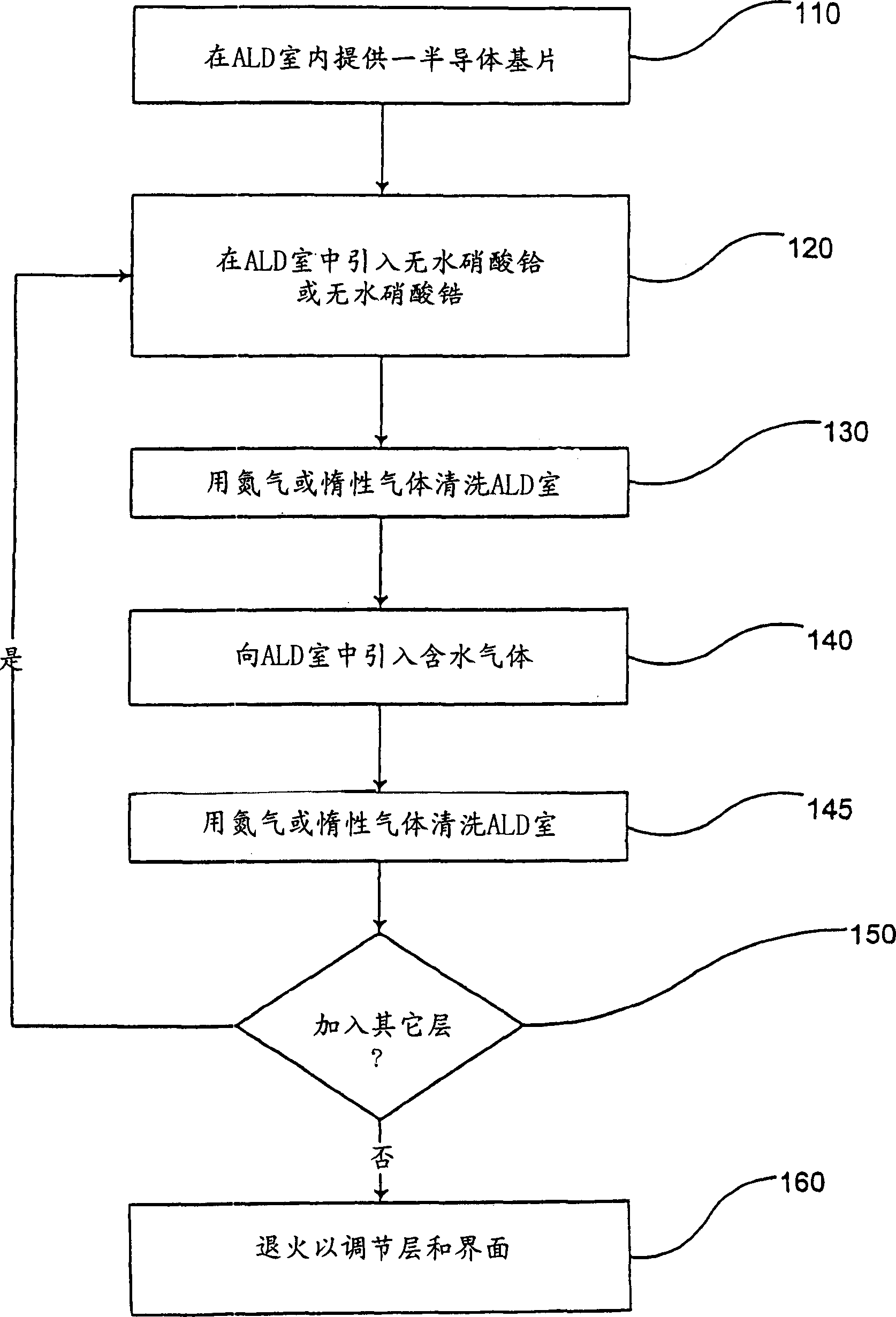
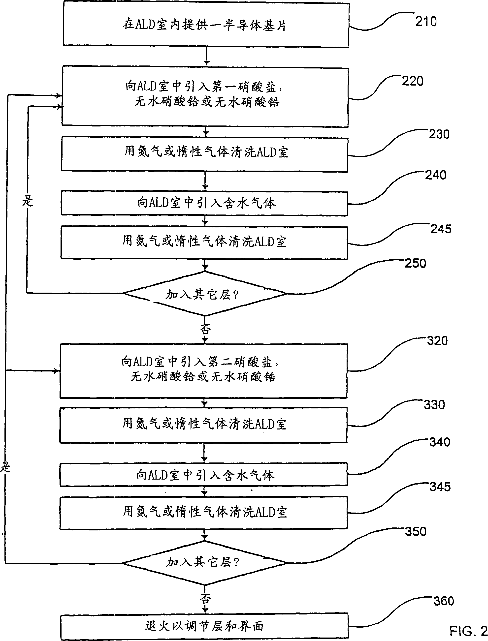
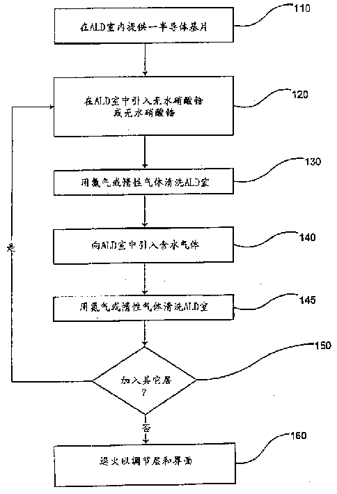
[0013] figure 1 is to illustrate the deposition of HfO 2 or ZrO 2 Flowchart of the thin film method steps. Step 110 provides a semiconductor substrate within an ALD chamber. Commercial ALD tools are currently available. An ALD tool, type F120, manufactured by Microchemistry Ltd. of Finland (now a division of ASM), can be used in the methods described herein. In a preferred embodiment, the semiconductor substrate has a hydrogen-terminated silicon surface. Although the method described here is particularly suitable for addressing the deposition of HfO on hydrogen-terminated silicon surfaces 2 or ZrO 2 problem, but it is also perfectly possible to use this method on other surfaces, including silicon dioxide, silicon oxynitride, SiGe surfaces and surfaces such as ZrSiO 4 and HfSiO 4 Depositing HfO on such a silicate 2 or ZrO 2 .
[0014] The semiconductor substrate is heated to a certain temperature to form the atomic layer deposition range. For example, when using anh...
PUM
| Property | Measurement | Unit |
|---|---|---|
| density | aaaaa | aaaaa |
Abstract
Description
Claims
Application Information