Eureka AIR delivers breakthrough ideas for toughest innovation challenges, trusted by R&D personnel around the world.

Nmos metal gate materials, manufacturing methods, and equipment using CVD and ald processes with metal based precursors

a technology of metal gate electrodes and manufacturing methods, which is applied in the direction of chemical vapor deposition coatings, coatings, semiconductor devices, etc., can solve the problems of many cvd processes producing less than desired, tantalum materials only being scarcely used for metal gate electrode formation, and less than desirable electronic properties of materials used for gate electrodes

Active Publication Date: 2011-10-27
APPLIED MATERIALS INC
View PDF8 Cites 311 Cited by
  • Summary
  • Abstract
  • Description
  • Claims
  • Application Information

AI Technical Summary

Problems solved by technology

However, the materials used for gate electrodes have had less than desirable electronic properties.
While tantalum materials have been used in semiconductor structures, such as barrier layers, tantalum materials have only been scarcely used for the formation of metal gate electrodes, despite the variety of electronic characteristics available from tantalum materials.
Advancement in technologies for forming semiconductor structures will now require conformal deposition on the bottom and side walls for work function materials on high k dielectric materials and gate electrodes on work function materials as opposed to the traditionally bottom only deposition approach making PVD undesirable and many CVD processes producing less than desired results.
Further, it is believed that PVD processes may have reached a limit at this size and aspect ratio.
Also, the variety of compositions for tantalum materials is very limited when using a PVD process.
Processes using TaCl5 may also suffer from chlorine contaminants within the tantalum material.
While metal-organic tantalum precursors may be used to form tantalum materials containing no chlorine contaminants, the deposited materials may suffer with the undesirable characteristic of a high carbon content.
Other metal materials to be deposited for metal gate electrodes have experienced similar difficulties as the deposition of tantalum.

Method used


Image

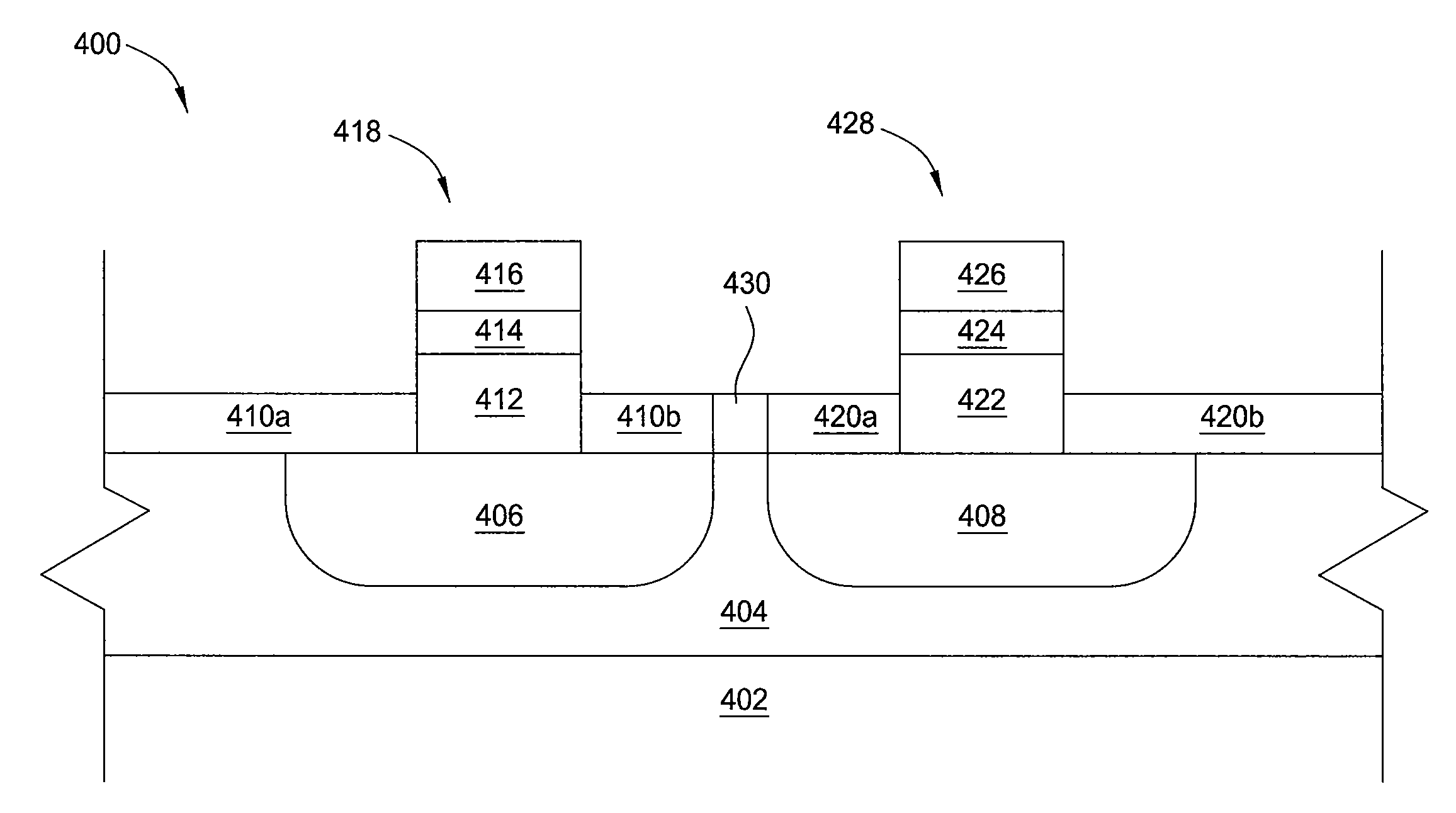
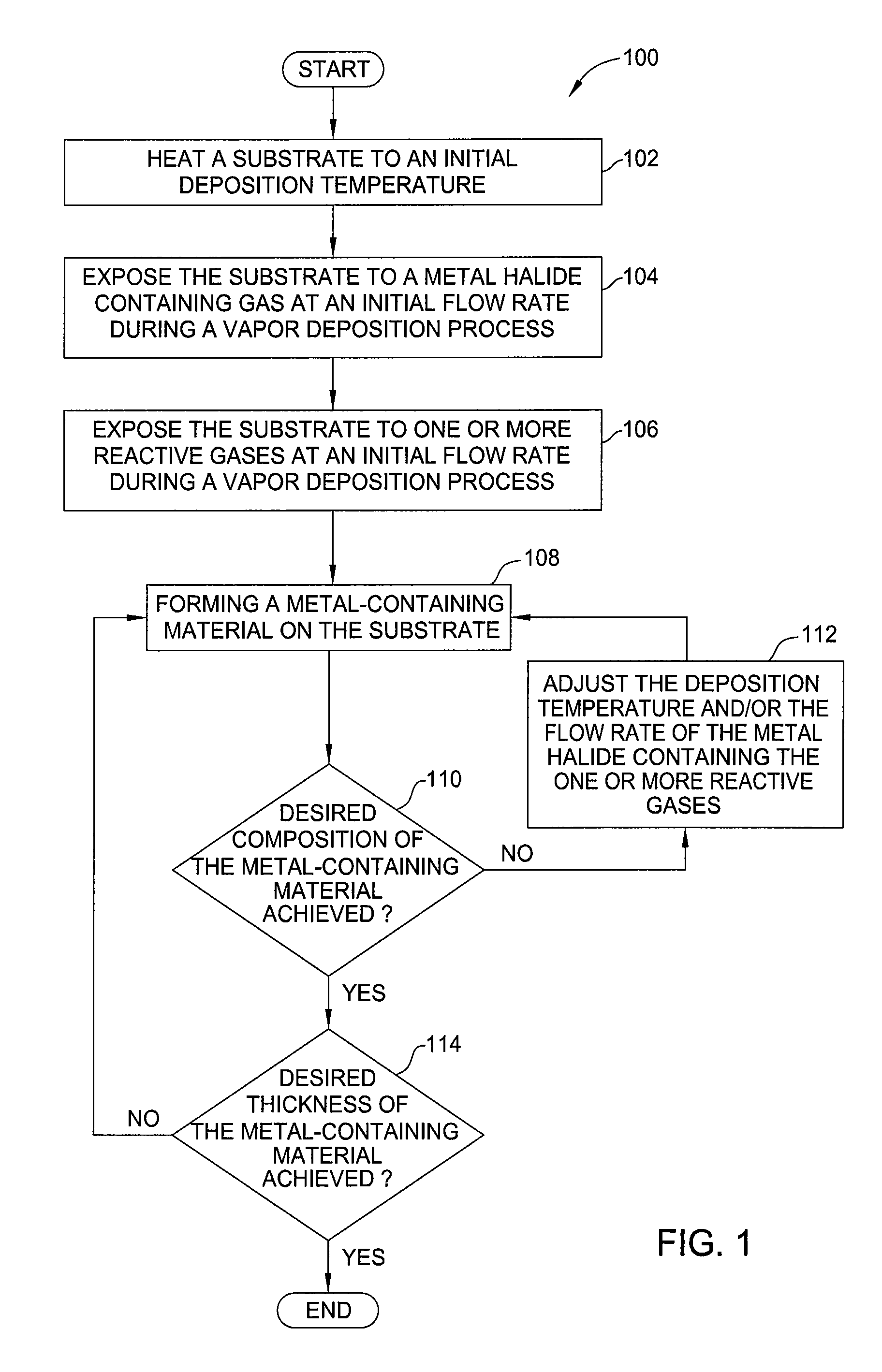
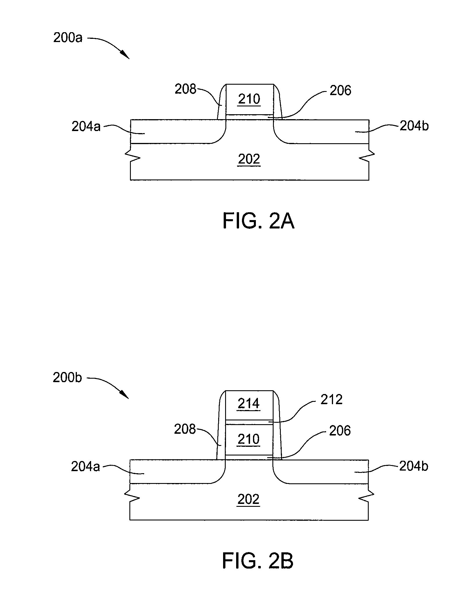
  • Nmos metal gate materials, manufacturing methods, and equipment using CVD and ald processes with metal based precursors
  • Nmos metal gate materials, manufacturing methods, and equipment using CVD and ald processes with metal based precursors
  • Nmos metal gate materials, manufacturing methods, and equipment using CVD and ald processes with metal based precursors

Examples


example 1

[0103]PE-ALD—A tantalum layer may be deposited on a substrate by a PE-ALD process. The substrate and the substrate pedestal were heated to a temperature of about 250° C. The substrate was sequentially exposed to a tantalum halide precursor, TaF5, an argon purge gas, a hydrogen plasma gas and a plasma is generated, and the argon purge gas during a PE-ALD cycle. The PE-ALD cycle exposed the substrate to the tantalum precursor gas for about 5 seconds, and the purge gas for about 2 seconds, and a hydrogen gas in which a plasma was generated at 400 watts and exposed the substrate for 10 seconds. The tantalum precursor gas had a flow rate of about 3 sccm of TaF5 in about 250 sccm of argon carrier gas. The tantalum material was deposited on the substrate to a final thickness of about 10 Å by 20 cycles of about 0.5 Å with each cycle lasting about 20 seconds.

[0104]The composition analysis of the tantalum material provided a resistivity of less than 200 μΩ-cm, such as from 130 μΩ-cm to less t...

example 2

[0105]ALD—A hafnium aluminide carbide layer may be deposited on a substrate by an ALD process. The substrate and the substrate pedestal were heated to a temperature of about 500° C. The substrate was sequentially exposed to a hafnium halide precursor, HfCl4, a nitrogen purge gas, an aluminum precursor, triethylaluminum (TEA), tritertbutyl aluminum (TTBA), and / or trimethylaluminum (TMA) and a second nitrogen gas purge during an ALD cycle. The ALD cycle exposed the substrate to the hafnium precursor gas for about 10 seconds, a nitrogen gas purge for 10 seconds, exposed the substrate to TEA and / or TTBA for 5 seconds, and then a nitrogen gas purge for 5 seconds. The hafnium precursor gas had a flow rate of about 2 sccm of HfCl4 in about 250 sccm of argon carrier gas. The TEA and / or TTBA precursor had a flow rate of about 30 mg / minute. The hafnium alumunide material was deposited on the substrate to a final thickness of about 2 to 3 Å by 100 cycles of about 200 to about 300 Å with each c...

example 3

[0106]PE-ALD—A hafnium aluminide layer may be deposited on a substrate by an ALD process. The substrate and the substrate pedestal were heated to a temperature of about 500° C. The substrate was sequentially exposed to a hafnium halide precursor, HfCl4, a nitrogen purge gas, an aluminum precursor, triethylaluminum (TEA) and / or tritertbutyl aluminum (TTBA), and a second nitrogen gas purge, during an ALD cycle, and a plasma of hydrogen after one or more of the ALD cycles. The ALD cycle exposed the substrate to the hafnium precursor gas for about 10 seconds, a nitrogen gas purge for 10 seconds, exposed the substrate to TEA and / or TTBA for 5 seconds, and then a nitrogen gas purge for 5 seconds. The hafnium precursor gas had a flow rate of about 2 sccm of HfCl4 in about 250 sccm of argon carrier gas. The aluminum precursor had a flow rate of about 30 mg / minute. The plasma gas was introduced at a flow rate of 2000 sccm and a plasma generated for about 10 seconds.


PUM

PropertyMeasurementUnit
work functionaaaaaaaaaa
temperatureaaaaaaaaaa
sizeaaaaaaaaaa

Abstract

Embodiments of the invention generally provide methods for depositing metal-containing materials and compositions thereof. The methods include deposition processes that form metal, metal carbide, metal silicide, metal nitride, and metal carbide derivatives by a vapor deposition process, including thermal decomposition, CVD, pulsed-CVD, or ALD. In one embodiment, a method for processing a substrate is provided which includes depositing a dielectric material having a dielectric constant greater than 10, forming a feature definition in the dielectric material, depositing a work function material conformally on the sidewalls and bottom of the feature definition, and depositing a metal gate fill material on the work function material to fill the feature definition, wherein the work function material is deposited by reacting at least one metal-halide precursor having the formula MXY, wherein M is tantalum, hafnium, titanium, and lanthanum, X is a halide selected from the group of fluorine, chlorine, bromine, or iodine, and y is from 3 to 5.

Description

CROSS-REFERENCE TO RELATED APPLICATIONS[0001]This application claims benefit of U.S. Provisional Patent Application Ser. No. 61 / 327,995 (APPM / 014327L), filed Apr. 26, 2010, which is herein incorporated by reference.BACKGROUND OF THE INVENTION[0002]1. Field of the Invention[0003]Embodiments of the invention generally relate to electronic device processing, and more particularly, to vapor deposition processes for metal-containing materials and the compositions of the metal-containing materials.[0004]2. Description of the Related Art[0005]The electronic device industry and the semiconductor industry continue to strive for larger production yields while increasing the uniformity of layers deposited on substrates having increasingly larger surface areas. These same factors in combination with new materials also provide higher integration of circuits per unit area on the substrate. As circuit integration increases, the need for greater uniformity and process control regarding layer charac...

Claims


Application Information

Patent Timeline
Patent Type & Authority Applications(United States)
IPC IPC(8): H01L21/3205
CPCC23C16/06H01L21/28008C23C16/42C23C16/45542H01L21/28079H01L21/28088H01L21/28097H01L21/28562H01L21/76843H01L21/76871H01L21/823814H01L21/823842H01L29/495H01L29/4966C23C16/32H01L29/49
Inventor GANGULI, SESHADRIGANDIKOTA, SRINIVASLEI, YULU, XINLIANGYU, SANG HOKIM, HOONMA, PAUL F.CHANG, MEIMAHAJANI, MAITREYEELIU, PATRICIA M.
Owner APPLIED MATERIALS INC
Why Eureka
Eureka Blog
Learn More