Method for making non-volatile memory with shallow junction

A non-volatile, manufacturing method technology, applied in semiconductor/solid-state device manufacturing, electrical components, circuits, etc., can solve the problem that the source/drain extension region is difficult to maintain, and achieve the effect of eliminating performance reduction and slowing down damage

Inactive Publication Date: 2003-05-21
MACRONIX INT CO LTD
View PDF0 Cites 2 Cited by
  • Summary
  • Abstract
  • Description
  • Claims
  • Application Information

AI Technical Summary

Problems solved by technology

This diffusion often causes the source / drain extensions to extend vertically into the semiconductor substrate, making shallow source / drain extensions difficult to maintain

Method used


Image

  • Method for making non-volatile memory with shallow junction
  • Method for making non-volatile memory with shallow junction
  • Method for making non-volatile memory with shallow junction

Examples


Embodiment Construction

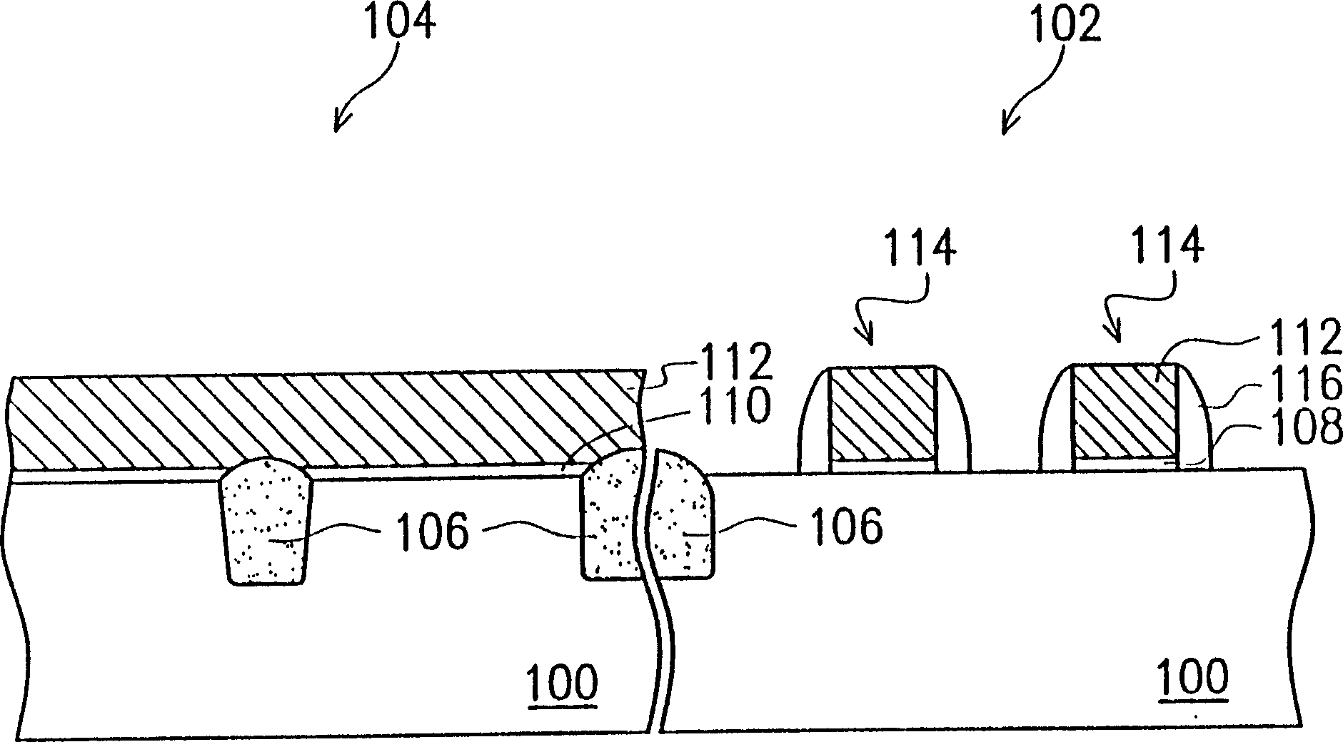
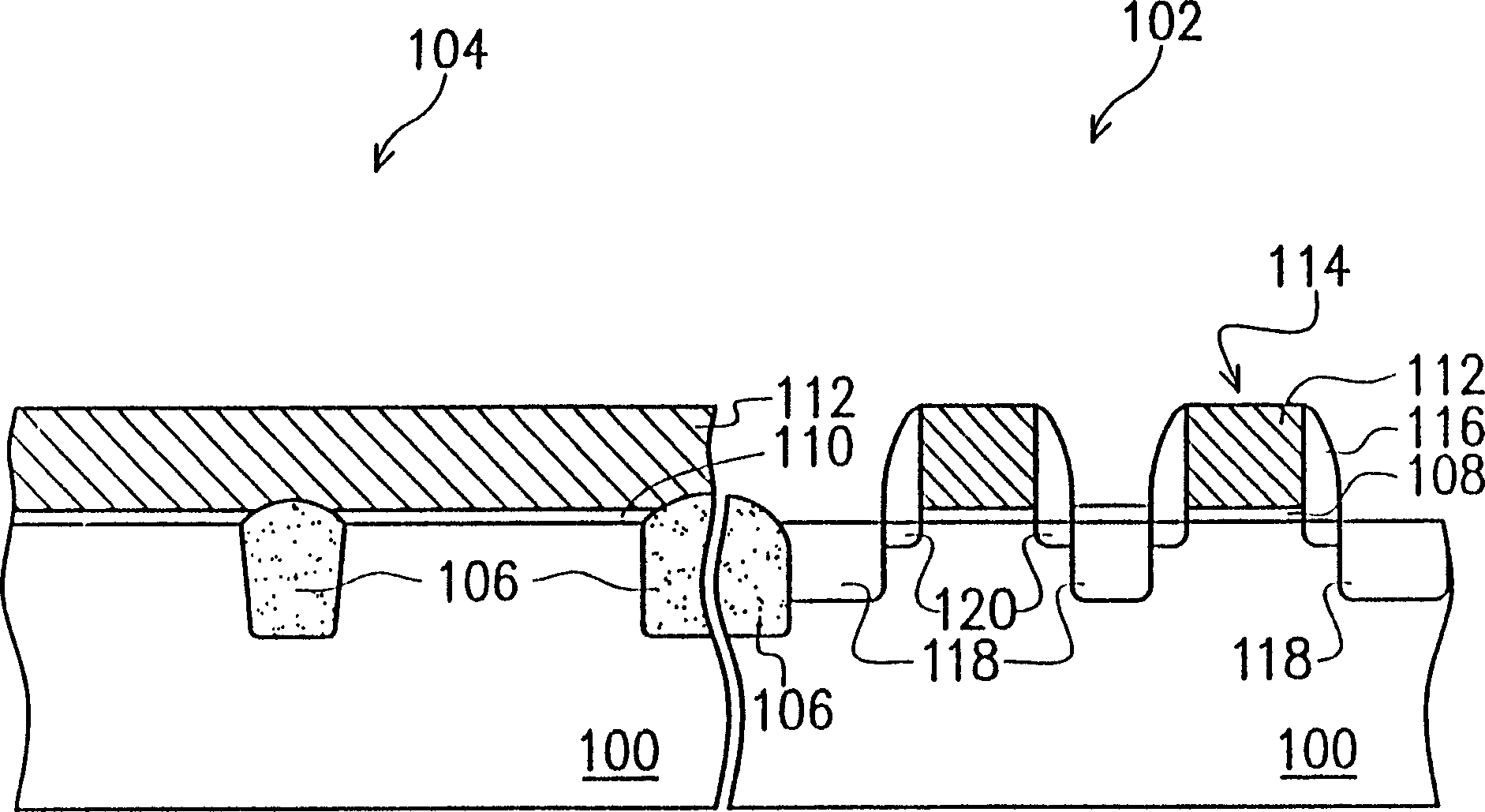
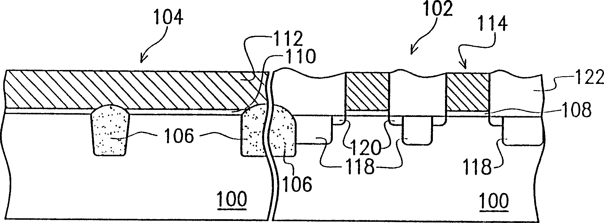
[0033] Embodiments of the present invention relate to a method of fabricating a non-volatile memory with shallow source / drain extensions, which can eliminate or reduce various problems in conventional methods.

[0034] Figures 1A-1E It is a cross-sectional view of manufacturing an embedded non-volatile memory according to an embodiment of the present invention. Such as Figure 1A As shown, the substrate 100 includes a memory cell region 102 and a peripheral circuit region 104, and isolation structures 106 are used to isolate the memory cell region 102, the peripheral circuit region 104 and other components. . The isolation structure 106 is, for example, a field oxide (FOX) or a shallow trench isolation (STI). A silicon monoxide / silicon nitride / silicon oxide (oxide / nitride / oxide, ONO) layer 108 is formed in the memory cell region 102 . The method for forming the silicon oxide / silicon nitride / silicon oxide layer 108 is, for example, sequentially forming a silicon oxide layer...


PUM


Abstract

A manufacturing method of the non-volatile memory having a shallow junction includes a grid structure on the substrate and the grid structure coprises an electron-catching layer and a conducting layer. A doped gap wall is formed on the side wall of the gap structure and then a plurality of embedding wires are formed in the substrate beside the grid structure. Further, the heat treatment is performed so that the dopant can diffuse into the substrate near the embedding wire through the doping gap wall.

Description

technical field [0001] The present invention relates to a method of manufacturing an integrated circuit device, and more particularly to a method of manufacturing a non-volatile memory with a shallow junction. Background technique [0002] Memory components can be widely used in many ways. Usually, a memory device includes thousands of memory cells, and these memory cells are arranged in rows and columns to form an array. In the memory cell array, the memory cells in the same row or column are connected by a common wire, and this common wire is called a word line; and the vertical wire related to data transmission is called a bit line. (bit line). The common structure of a memory device consists of an array of memory cells, each of which is located at the intersection of a parallel array of buried wires formed in a semiconductor substrate and a vertical array of wires formed on the substrate (intersection) on. Such a memory structure is, for example, a read-only memory (...

Claims


Application Information

Patent Timeline
Patent Type & Authority Applications(China)
IPC IPC(8): H01L21/8246
Inventor 郭东政黄守伟刘建宏潘锡树
Owner MACRONIX INT CO LTD
Why Eureka
Try Eureka