Solid-state imaging device and its mfg. method

A solid-state imaging device, solid-state technology, applied in radiation control devices, semiconductor/solid-state device parts, installations, etc., can solve the problems of production decline, hinder production improvement, and easy cracking of solid-state imaging components, and achieve connection failure. reduced effect

Inactive Publication Date: 2003-07-09
PANASONIC CORP
View PDF1 Cites 5 Cited by
  • Summary
  • Abstract
  • Description
  • Claims
  • Application Information

AI Technical Summary

Problems solved by technology

[0010] In various methods, due to the thermal deformation of the 3D printed circuit board, the bonding of the solid-state imaging element is extremely prone to cracking, which will lead to a decrease in production yield
[0011] When the printed circuit board is made into a three-dimensional structure, but its thermal deformation is three times that of the conventional two-dimensional structure, there is a serious problem that the deformation due to the difference in expansion coefficient hinders the increase in yield

Method used


Image

  • Solid-state imaging device and its mfg. method
  • Solid-state imaging device and its mfg. method
  • Solid-state imaging device and its mfg. method

Examples


Embodiment 1

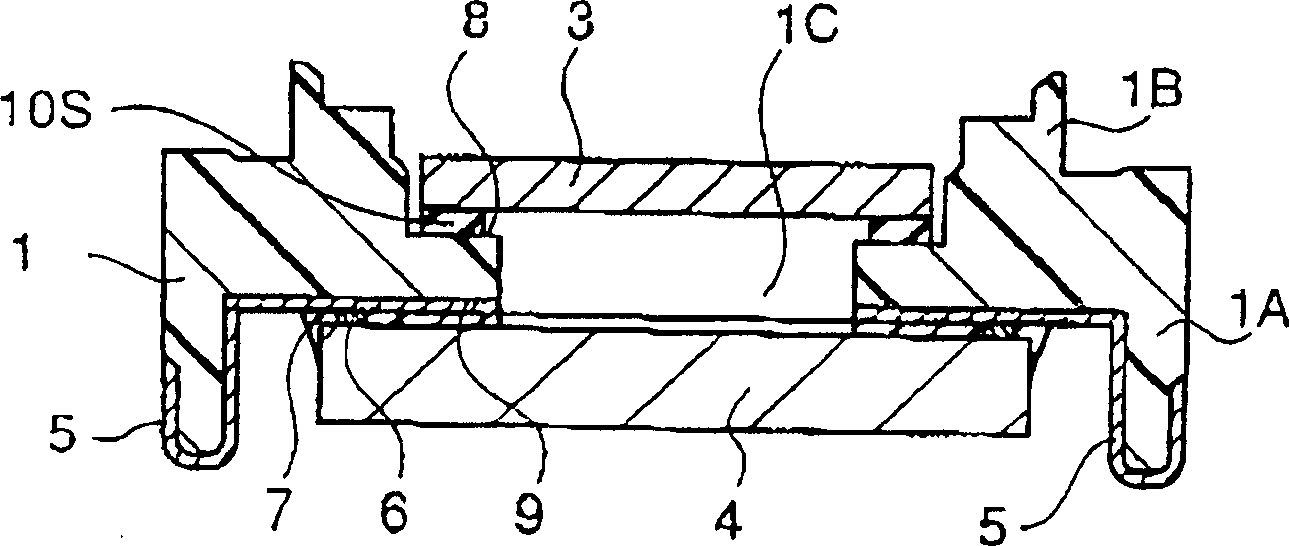
[0108] figure 1 is a view of the main body portion of the solid-state imaging device of the first embodiment of the present invention.

[0109] In the solid-state imaging device of the first embodiment, when the solid-state imaging element 4 is connected to the resin structural member 1 having the wiring portion, the structural member 1 is formed such that the optical filter 3 passes through a ceramic plate having a thermal expansion coefficient smaller than that of the resin structural member 1 10S and connected to the filter mounting surface 8 of the resin structure 1.

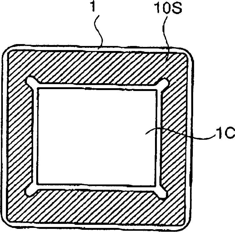
[0110] Such as figure 2 As shown, a ceramic plate 10S is used as a fixing member having a rectangular ring shape with a thickness of about t=0.1-0.2 mm and a coefficient of thermal expansion of about 10 ppm / °C. The ceramic plate is composed of insulating polyphthalamide resin. The image forming apparatus includes: a resin structural member 1 comprising, a leg portion 1A having a rectangular truncated sha...

Embodiment 2

[0122] Below, refer to Figure 5 A second embodiment of the present invention will be described.

[0123] In the solid-state imaging device of the second embodiment, the structural member 1 is integrally molded, and the metal plate 10M is sandwiched in the resin structural member 1 . In this embodiment, the structural member 1 is integrally molded and the metal plate 10M is clamped in the structural member 1. The surfaces of the metal plate 10M are in contact.

[0124] In solid-state imaging devices such as Figure 5 As shown, a metal plate 10M having a rectangular ring shape is integrally molded between the filter mounting surface 8 and the solid-state image pickup element mounting surface 9 of the resin structural member 1 having a wiring portion made of thermoplastic PPS resin in parallel Because of these surfaces, deformation of the solid-state imaging element mounting surface 9 is suppressed.

[0125] Other parts are formed in the same manner as the first embodiment. ...

Embodiment 3

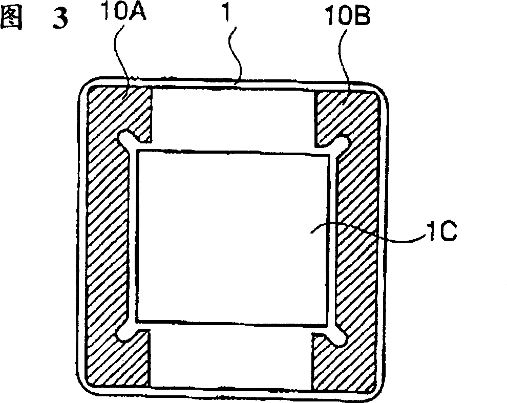
[0134] Below, refer to Figure 7 A third embodiment of the present invention will be described.

[0135] In the second embodiment, the structural member 1 is formed by integral molding in which a metal plate 10M is sandwiched in the resin structural member 1 and the back of the optical filter 3 is formed with the metal plate 10M sandwiched in the resin structural member 1 surface contact. In this example, as Figure 7 As shown, the ceramic plate 10S is sealed into the resin structure 1 except for the side facing the through portion 1C. However, the ceramic plate 10S can also be completely sealed into the structure 1 .

[0136] Other parts are formed in the same manner as the second embodiment. Like parts use the same reference numerals.


PUM


Abstract

A solid-state imaging apparatus includes: a resin structure member configured by an insulating resin and having a through-opening portion a wiring portion is formed on the surface of the resin structure member; a solid-state image pickup element connected to the wiring portion and attached to the through-opening portion; and a light-transmitting member disposed to cover the through-opening portion with being separated from the solid-state image pickup element by a predetermined distance. A fixing member which is smaller in coefficient of thermal expansion than the insulating resin is placed in close proximity to a solid-state image pickup element attaching face.

Description

technical field [0001] The present invention relates to a solid-state imaging device and a manufacturing method thereof, and more particularly to a small-sized imaging device having a solid-state imaging element such as a surveillance camera, a medical camera, or a vehicle-mounted camera and a manufacturing method thereof. Background technique [0002] Such an imaging device receives an image through an optical system such as a lens, and outputs the image in the form of an electric signal. In recent years, with the miniaturization and performance improvement of such imaging devices, and the decreasing size of video cameras, the imaging devices are used in various fields and their market is expanding to image input devices. [0003] In a conventional imaging device using a solid-state image pickup element, each component such as a lens, a solid-state image pickup element, and an LSI mounted with a drive circuit for the image pickup element and a signal processing circuit has ...

Claims


Application Information

Patent Timeline
Patent Type & Authority Applications(China)
IPC IPC(8): H01L27/146H01L31/0203H01L31/0232H04N5/225
CPCH01L27/14618H01L31/0203H01L31/0232H04N5/2253H01L2924/0002H01L31/02325H04N23/54H01L2924/00H01L27/146H01L23/02
Inventor 原园文一高出芳治
Owner PANASONIC CORP
Why Eureka
Try Eureka