

Mask and its mfg. method, electroluminance device and its mfg. method and electronic machine
一种制造方法、掩模的技术,应用在电致发光光源、照明装置、光机械设备等方向,能够解决很难制造高精密的掩模等问题,达到掩模图形高精密的效果
- Summary
- Abstract
- Description
- Claims
- Application Information
AI Technical Summary
Problems solved by technology
Method used
Image

Examples
Embodiment 1
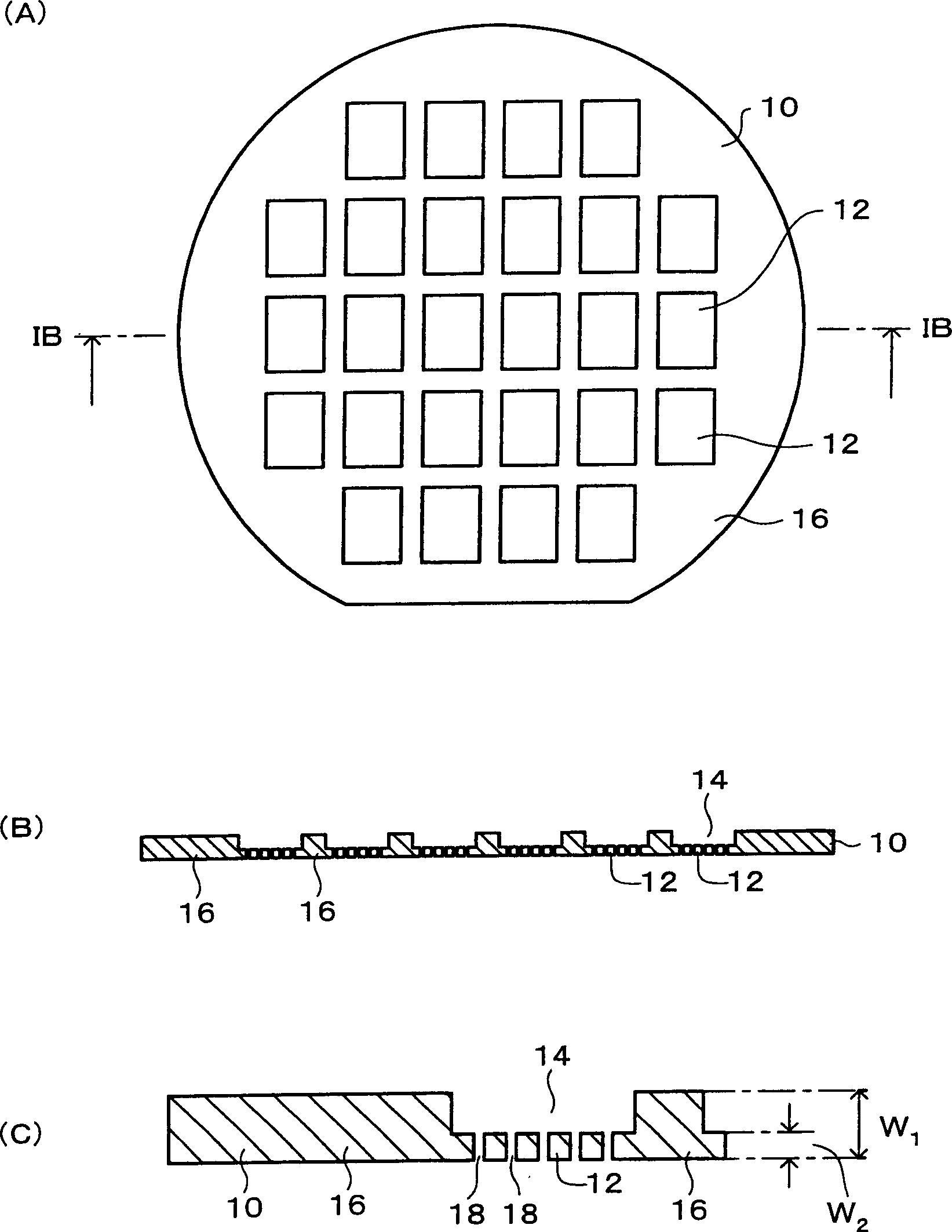
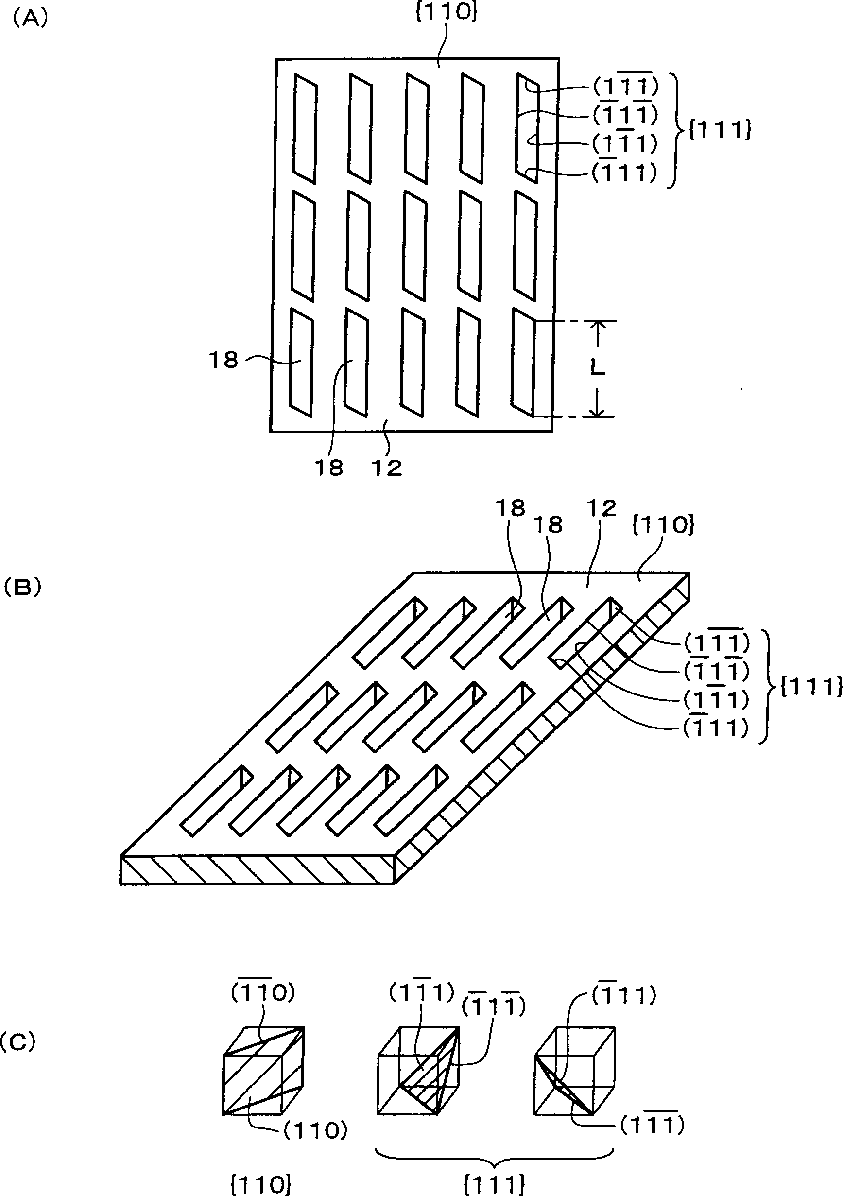
[0070] figure 1 A to 1C are diagrams illustrating masks according to examples of the present invention. figure 1 B is figure 1 The cross-sectional view of line IB-IB shown in A, figure 1 C is figure 1 Partial enlarged view of B. The mask has a single crystal substrate 10 (or consists of only the single crystal substrate 10). The single crystal substrate 10 is, for example, a single crystal silicon substrate, but may also be a silicon wafer. Single crystal substrate 10 has a surface represented by a specular index {110}. For example, the surface and the back surface of the single crystal substrate 10 are {110} planes. It should be noted that the {110} plane includes multiple planes equivalent to the (110) plane. In a cubic lattice, the direction perpendicular to the {110} planes is the orientation.
[0071] At least one (for example, a plurality of) thin-walled portion 12 is formed on single crystal substrate 10 . The plurality of thin portions 12 may be arranged in a...
Embodiment 2
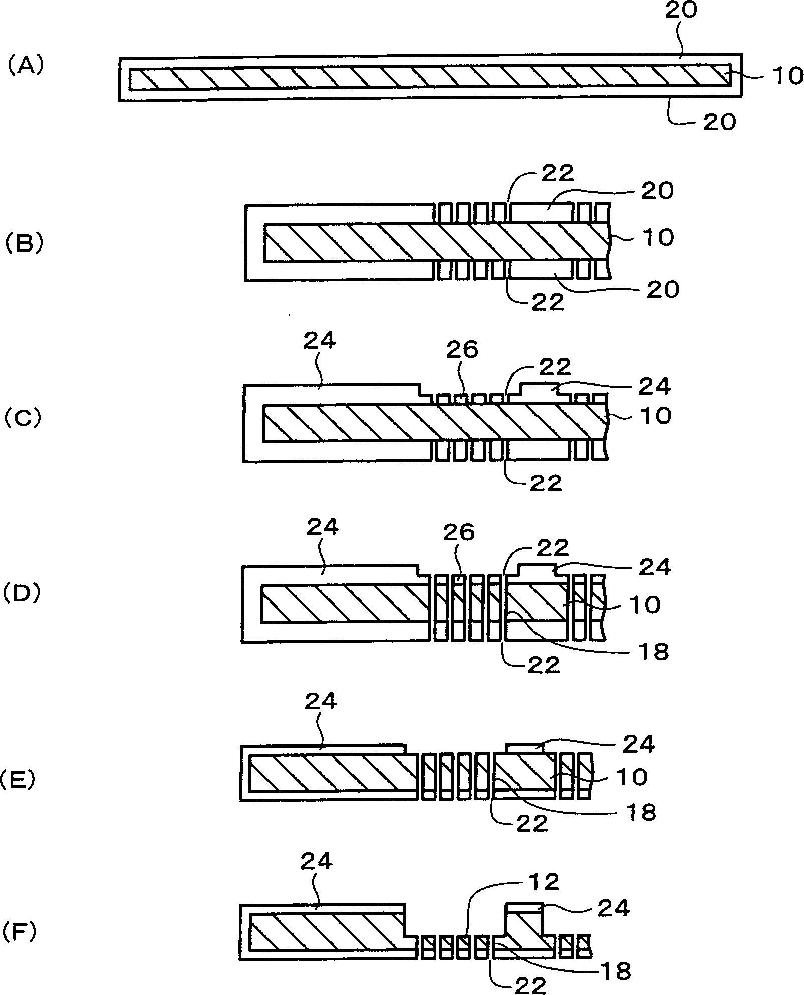
[0092] Figure 4 A to 4C are diagrams illustrating a method of manufacturing the mask of Example 2. In Example 1, openings 22 are formed in etching-resistant film 20 on both surfaces of single crystal substrate 10 . At this time, since the alignment of the openings 22 on both sides is difficult, the following description will focus on a method for easily performing the alignment.
[0093] Such as Figure 4 As shown in A, a first opening 34 is formed in the etch-resistant film 30 formed on one surface of the single crystal substrate 10, and a second opening 36 is formed in the etch-resistant film 32 formed on the other surface. Here, the widths of the first and second openings 34, 36 have the following relationship:
[0094] B Figure 4 As shown in B, etching is carried out as Figure 4 As shown in C, a through hole 38 is formed. Such as Figure 4 As shown in C, the end of the etch-resistant film 32 where the small-sized second opening 36 is formed protrudes toward the ins...
Embodiment 3
[0096] Figure 5 It is a figure explaining the manufacturing method of the mask of Example 3. In Example 1, the thickness W of the single crystal substrate 10 1 (refer to figure 1 C) and the length L of the long side of the parallelogram of the opening 22 of the etch-resistant film 20 (with figure 2The length L of the long side of the parallelogram of the through hole 18 shown in A is the same) has the following relationship:
[0097] √3×W 1 <L If it is such a relatively thin single crystal substrate, a through hole can be formed, but for a thicker single crystal substrate, etching stops halfway, and a through hole cannot be formed.
[0098] A method of forming a through-hole when the following relationship holds true in this embodiment (when the single crystal substrate is thick) will be described.
[0099] √3×W 1 ≥ L
[0100] Such as Figure 5 As shown, small through holes (holes smaller than the through holes) 42 are formed before etching in the region where the th...
PUM
 Abstract
Description
Claims
Application Information