EEPROM memory chip with multiple use pinouts
A storage chip and chip technology, applied in information storage, static memory, read-only memory, etc., can solve unrealistic problems and achieve the effect of reducing the number of pins
- Summary
- Abstract
- Description
- Claims
- Application Information
AI Technical Summary
Problems solved by technology
Method used
Image

Examples
Embodiment Construction
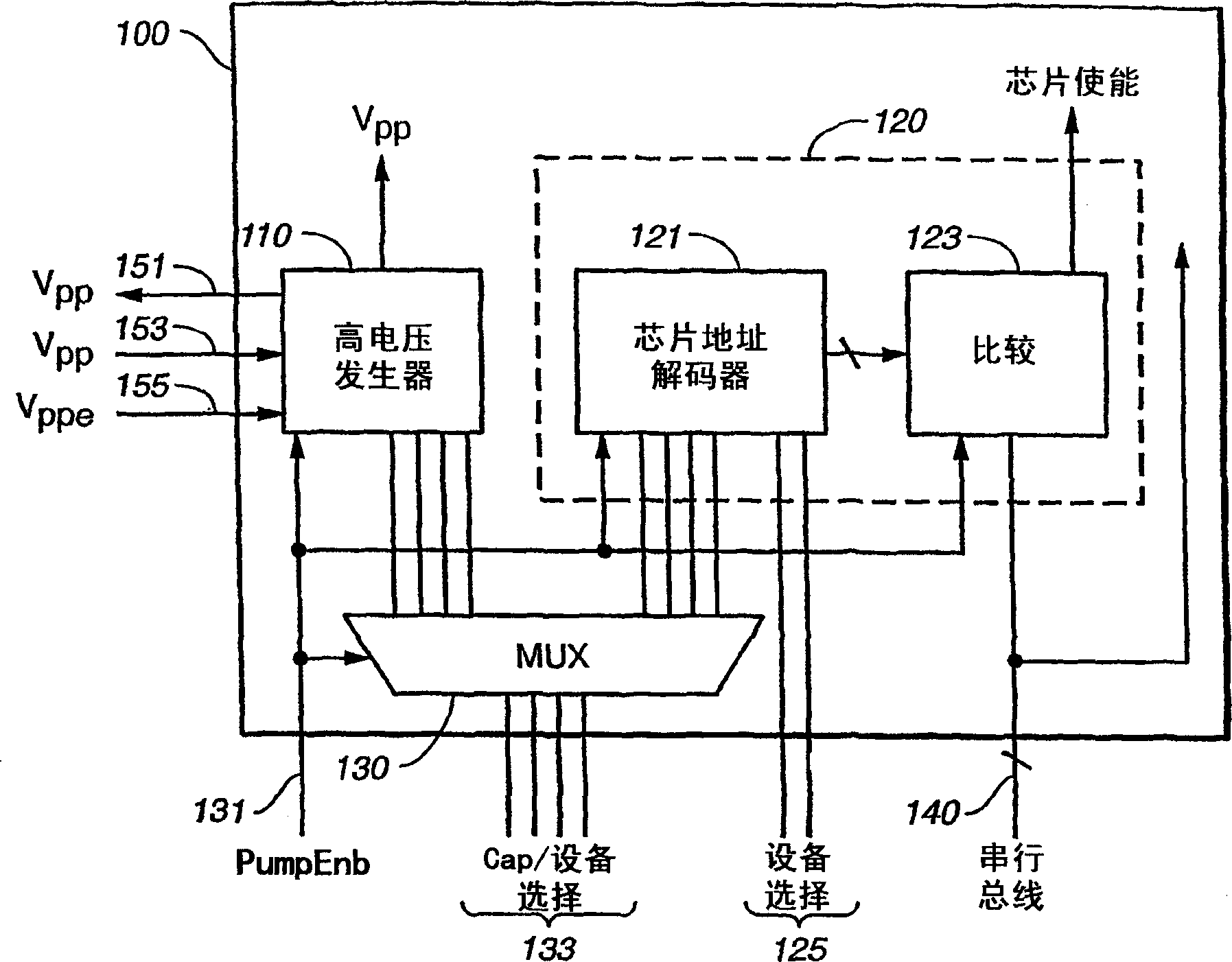
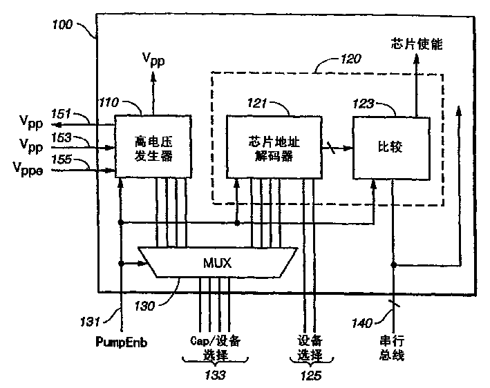
[0012] figure 1 It is a typical embodiment that includes many aspects of the present invention. It is a partial block diagram of a non-volatile memory chip 100 used in the system described in the pending U.S. patent application entitled "Flash EEPROM System with Simultaneous Multiple Data Sector Programming and Storage of Physical Block Characteristics in Other Designated Blocks (Flash EEPROM system capable of simultaneously programming multiple data areas and storing physical block characteristics in other designated blocks)", and has been included in the above reference. The chip includes a high voltage generator 110 , a multiplexing circuit / input buffer MUX 130 , and a device selection circuit 120 including a chip address decoder 121 and a comparison module 123 . Other peripheral components and the actual bank of memory cells have been removed to simplify the discussion. Also, only those inputs corresponding to the pins discussed below are explicitly labeled, while other...
PUM
 Abstract
Description
Claims
Application Information