Method for producing miro display

A technology of micro-display and manufacturing method, which is applied in the fields of instruments, nonlinear optics, optics, etc., and can solve the problems of high product cost, increased probability of waste, and difficulty of adding micro-displays, etc.

Inactive Publication Date: 2003-09-10
SINGAPORE UNITED PROJECTION
View PDF0 Cites 15 Cited by
  • Summary
  • Abstract
  • Description
  • Claims
  • Application Information

AI Technical Summary

Problems solved by technology

[0004] Therefore, it is obvious from the above-mentioned existing microdisplay manufacturing process that in this existing process, for all chips on the wafer, no matter whether they are qualified or invalid, they are all applied with sealing glue, sprinkling spacers, and combining ITO chips one by one. The process steps of glass sheet, vacuuming, injecting liquid crystal, sealing, cutting and testing will consume and invest more materials, man-hours and manpower, which will relatively increase the dif

Method used


Image

  • Method for producing miro display
  • Method for producing miro display
  • Method for producing miro display

Examples


Embodiment Construction

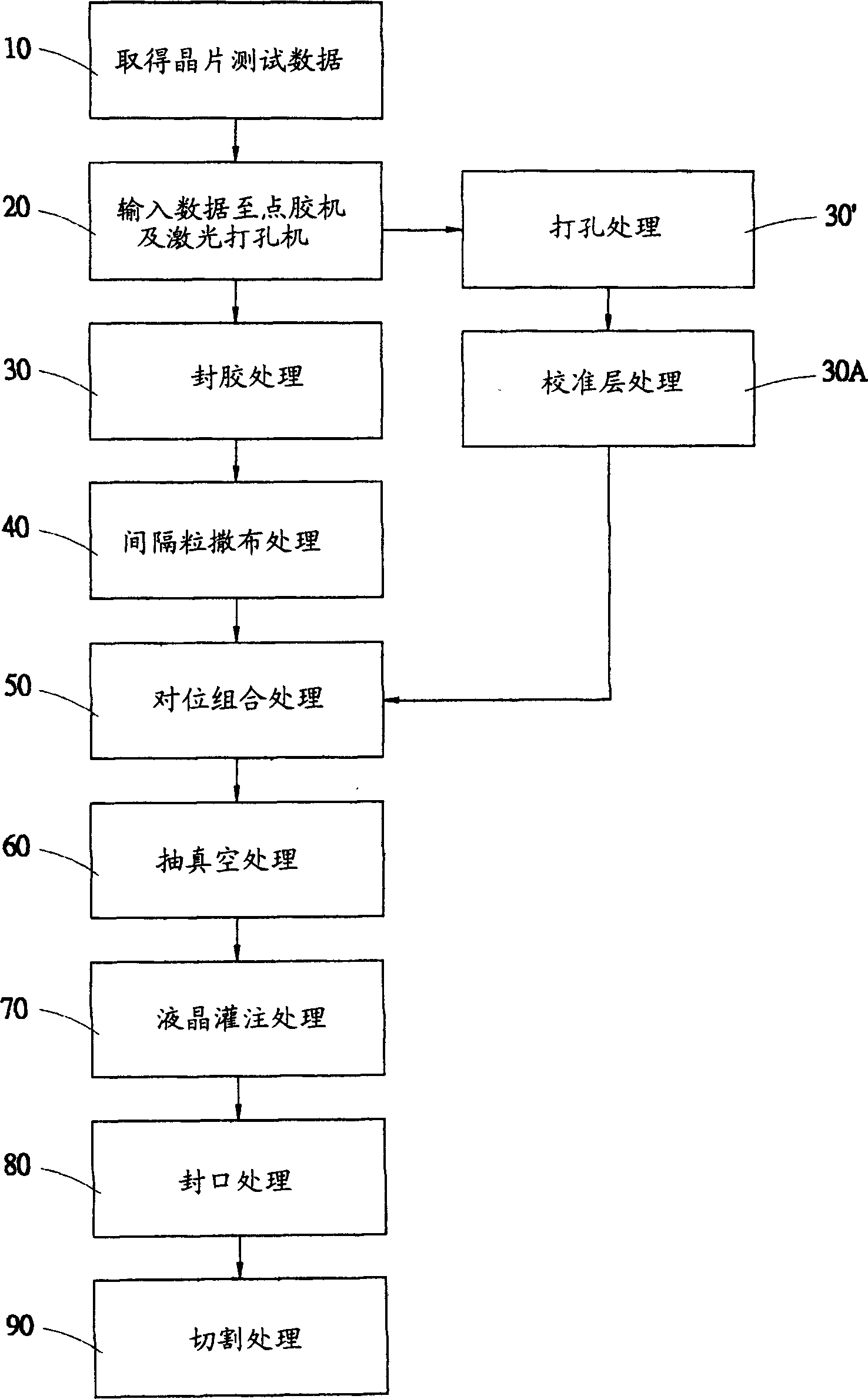
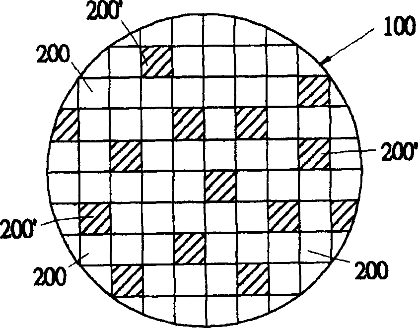
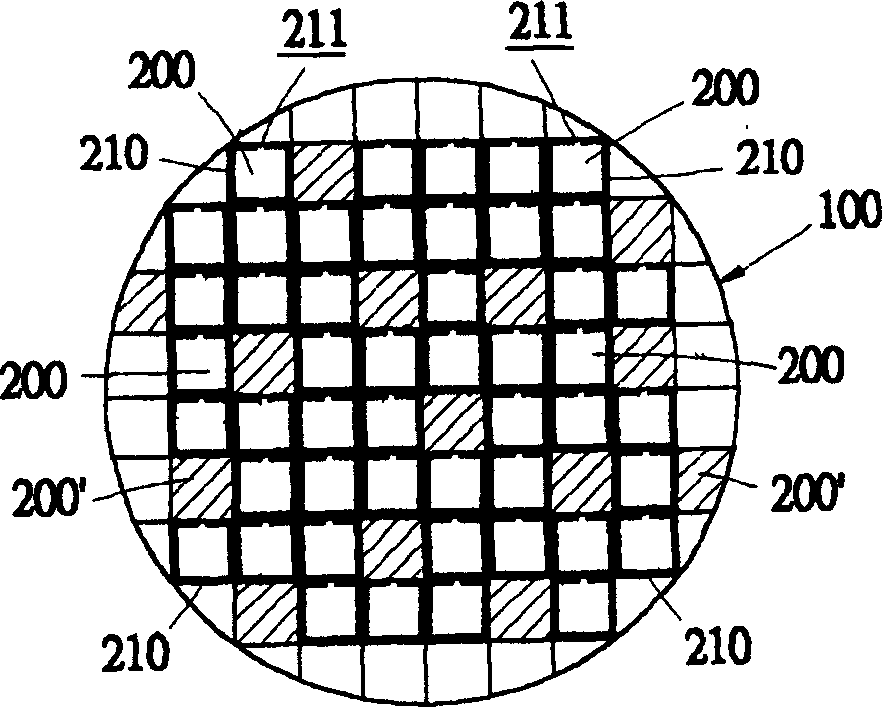
[0018] First, see figure 1 as shown, figure 1 and figure 2 Shown is the manufacturing process of the microdisplay of the present invention, wherein, shown in step 10 is to obtain the wafer test data, i.e. the wafer 100 as the basic circuit (such as figure 2 Shown) the test result data of each chip 200 and 200', this data source can be measured by the chip manufacturing plant, test plant or self-made chip test equipment, and the test methods are all in the needle test (PROB STATION) (not shown), and whether the needle measurement position is tested by moving the test head or moving the chip, the X-axis and Y-axis coordinate data and test results of the chip 200 and 200' will be Will be recorded one by one in detail with magnetic tape, magnetic disk or any other data type, and the wafer 100 disclosed in the present invention is the specification of 6 inches, 8 inches or 12 inches, and in the present invention then is with chip 200 is the test result "passed", and the chip 2...


PUM


Abstract

The manufacture of mniature LCD includes testing individual chips on the basic substrate, marking the useless chip after test, inputting the test data into one gluing machine or laser perforator, making glue frame, around the qualified chips in the gluing machine, perforating implanting holes on ITO glass in the positions corresponding to the qualified chips, spreading interval grains to the glued chip checkers, assembling ITO glass sheets onto the chips according to the tested data, injecting liquid crystal via the injecting holes in the ITO glass sheet over the qualified chips so as to make liquid crystal diffuse to between the chips and ITO glass sheet, sealing and cutting to make miniature LCD product with qualified chip. The product is then screened.

Description

(1) Technical field [0001] The invention relates to a manufacturing method of a microdisplay, in particular to a manufacturing technology of a microdisplay capable of screening base chips and simplifying and deleting the processing quantity of invalid chips. (2) Background technology [0002] Micro-display (MICRO-DISPLAY) is widely used in electrical projection display equipment such as liquid crystal projectors, computer monitors, projection TVs, etc. Its main function is to generate the original image of optical projection, and through each pixel (PIXEL) of the mirror The reflective function between the open (ON) or closed (OFF) control, cooperate with the optical projection light source and the optical projection mechanism composed of the lens group, so that the original image can be magnified and projected on the screen or display screen. Therefore, the application range of the micro-display is wide, and the number of its use in electrical appliances or optical projectio...

Claims


Application Information

Patent Timeline
IPC IPC(8): G02F1/1333
Inventor 曾令远郑浩民
Owner SINGAPORE UNITED PROJECTION
Why Eureka
Try Eureka