Optical modulator

A light modulator and gap technology, applied in the field of light modulators, can solve problems such as hindering the modulation speed

Inactive Publication Date: 2003-09-17
MITSUBISHI ELECTRIC CORP
View PDF0 Cites 1 Cited by
  • Summary
  • Abstract
  • Description
  • Claims
  • Application Information

AI Technical Summary

Problems solved by technology

It is considered that this problem prevents the realization of a low-chirp modulator that can be used at a very high-speed modulation rate of 40 Gbps. In fact, academically, no low-chirp modulation that can operate at 40 Gbps has been reported. device

Method used


Image

  • Optical modulator
  • Optical modulator
  • Optical modulator

Examples


no. 2 Embodiment

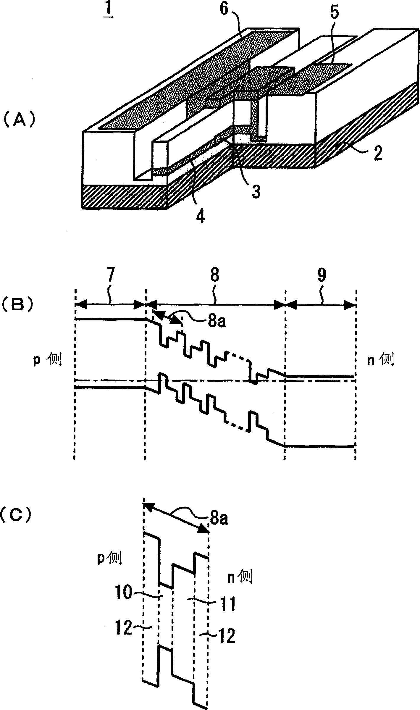
[0036] Figure 5 (A) and (B) are diagrams illustrating the energy bands of the multiple quantum wells of the optical modulator according to the second embodiment of the present invention. exist Figure 5 In, due to the use of figure 1 Portions with the same reference numerals denote the same components, and thus their descriptions are omitted. exist Figure 5 In (A), reference numeral 13 denotes a layer having a band gap between the band gap of the well layer 10 and the band gap of the intermediate layer 11 . exist Figure 5 In (B), reference numeral 14 denotes a layer having a gap between the gap of the intermediate layer 11 and the gap of the barrier layer 12 .

[0037] In the above-mentioned first embodiment, the quantum wells 8a of one period of the multiple quantum wells 8 have three types of layers: the well layer 10, the intermediate layer 11, and the barrier layer 12. In the second embodiment, the quantum well 8 a of one period may have four types of layers in w...

no. 3 Embodiment

[0041] Image 6 It is a diagram showing a semiconductor laser with an optical modulator (modulator-integrated semiconductor laser device) according to a third embodiment of the present invention; Image 6 Among them, the reference numeral 21 represents the optical modulator 1 etc. described in the first embodiment or the second embodiment, the reference numeral 22 represents the isolation (isolasion) region, the reference numeral 23 represents the semiconductor laser, and the reference numeral 24 represents the light modulator absorbing layer, Reference numeral 25 designates a semiconductor laser active layer, reference numeral 26 designates a diffraction grating, reference numeral 27 designates an InP substrate, and reference numeral 28 designates the entirety of a semiconductor laser with an optical modulator.

[0042] In this third embodiment, the optical modulator 1 of the above-mentioned first embodiment or the second embodiment is integrated with the semiconductor laser ...

no. 4 Embodiment

[0045] Figure 7 It is a diagram showing an optical amplifier-integrated optical modulator according to a fourth embodiment of the present invention. exist Figure 7 , due to the Image 6 Portions with the same reference numerals denote the same components, and thus their descriptions are omitted. exist Figure 7 Among them, reference numeral 32 denotes a (semiconductor) optical amplifier, reference numeral 33 denotes an optical amplifier active layer, and reference numeral 31 denotes the entirety of an optical amplifier-integrated optical modulator.

[0046] In this fourth embodiment, the semiconductor optical amplifier 32 can be integrated on the optical modulator 1 of the above-mentioned first embodiment or the second embodiment. The resulting loss is compensated.

[0047] If the fourth embodiment is adopted in the manner described above, by integrating the semiconductor optical amplifier 32 on the optical modulator 1 of the first embodiment or the second embodiment, o...


PUM


Abstract

An object of the present invention is to provide an optical modulator capable of reducing only a chirp without deteriorating extinction characteristics. Insert the intermediate layer (11) between the well layer (10) and the barrier layer (12) on the n side, apply tensile deformation to the well layer (10), and in the band gap Eb (eV) of the barrier layer (12), Between the band gap Ew (eV) of the well layer (10) and the band gap Em (eV) of the intermediate layer 11, the relationship of Ew<Em<Eb can be maintained. It is also possible to form a tensioned quantum well structure having four types of layers added with another layer on top of the tensioned quantum well structure having these three types of layers. The band gap of the other layer is the band gap between the well layer (10) and the intermediate layer (11), or the band gap between the intermediate layer (11) and the barrier layer (12). In the quantum well (8a) per one period, the number of layers is any number.

Description

technical field [0001] The invention relates to a light modulator, which has an absorption layer of multiple quantum wells between a p-type semiconductor and an n-type semiconductor. technical background [0002] An electric field absorption optical modulator (Electroabsorption Optical Modulator: EA modulator) utilizes an electric field absorption effect in which an optical absorption coefficient (hereinafter simply referred to as "absorption coefficient") changes due to an electric field acting on a substance. Specifically, the EA modulator performs optical modulation by applying an electric field to the semiconductor absorbing waveguide layer to change the absorption coefficient of the absorbing waveguide layer. waveguide, while using the type of bulk semiconductor layer. [0003] Figure 8 (A) and Figure 8 (B) shows the energy band (band) of the conventional EA modulator using the quantum well in the absorbing layer waveguide layer, Figure 8 (C) shows the energy band o...

Claims


Application Information

Patent Timeline
Patent Type & Authority Applications(China)
IPC IPC(8): G02F1/015G02F1/017
CPCB82Y20/00G02F1/01708G02F2203/25G02F1/01758G02F1/01766G02F1/0157G02F1/13
Inventor 宫崎泰典
Owner MITSUBISHI ELECTRIC CORP
Why Eureka
Try Eureka