EML chip structure with anti-reflection function and preparation method

A chip structure and anti-reflection technology, applied in the structure of optical resonant cavity, final product manufacturing, sustainable manufacturing/processing, etc., can solve optical disturbance, side mode suppression ratio, absorption curve and optical power influence, influence on optical power, etc. problem, to achieve the effect of reducing chirp, excellent anti-reflection, and enhancing anti-reflection characteristics

Inactive Publication Date: 2022-07-08
SHANXI YUANJIE SEMICONDUCTOR TECH CO LTD
View PDF4 Cites 1 Cited by
  • Summary
  • Abstract
  • Description
  • Claims
  • Application Information

AI Technical Summary

Problems solved by technology

Due to the hole stacking effect in the quantum well (QW) absorbing layer of the EAM, the EML frequency chirp increases with the increase of the EAM optical output power, thereby affecting the optical power
The second is the reflection of light in the EAM, which will cause corresponding optical disturbances. When high-speed modulation is used, it will affect the side mode suppression ratio, absorption curve and optical power.

Method used


Image

  • EML chip structure with anti-reflection function and preparation method
  • EML chip structure with anti-reflection function and preparation method
  • EML chip structure with anti-reflection function and preparation method

Examples


preparation example Construction

[0062] A preparation method of an EML chip with anti-reflection function, comprising:

[0063] On the InP substrate 1, the DFB quantum well 3 is grown by MOCVD deposition, the material used is InGaAsP, and the growth temperature is 600-800 degrees; using the photolithography technology, the grating layer 5 is etched on the DFB quantum well 3, and on the grating layer 5 The grating cover layer 13 is obtained by using the MOCVD growth technology, and the growth thickness is 100-200 nm.

[0064] Use vapor deposition to generate a SiyOx mask on the grating cover layer 13, x / y is between 1.5~2, use photolithography technology to etch the SiyOx mask layer and one end of the grating cover layer 13, use wet etching and dry The method is etched to stop at the bottom of the DFB quantum well 3 to obtain the first etched region 16 .

[0065] In the first etching region 16, the MOCVD selective region growth technology is used to grow the EAM quantum well 4; the EAM quantum well adopts a d...

Embodiment 1

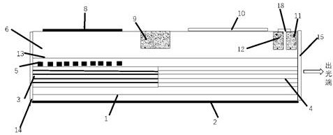
[0072] see Figure 4 , Figure 5 and Image 6 , using MOCVD to grow the DFB quantum well 3 on the InP substrate 1, the material used is InGaAsP, and the growth temperature is 750 degrees; using photolithography technology, the grating layer 5 is etched on the DFB quantum well, and the grating layer 5 is grown by MOCVD technology to obtain a grating cover layer 13 with a growth thickness of 150 nm.

[0073]A SiyOx mask layer is generated on the grating cover layer 13, x / y = 2, the SiyOx mask layer and one end of the grating cover layer 13 are etched using a photolithography technique, and wet etching and dry etching are used to etch to The bottom of the DFB quantum well 3 stops to obtain the first etching region 16; in the first etching region 16, the MOCVD selective region growth technology is used to grow the EAM quantum well 4;

[0074] In the first etching region 16, the MOCVD selective region growth technology is used to grow the EAM quantum well 4; the EAM quantum well...

Embodiment 2

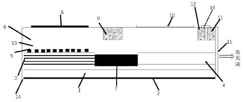
[0079] On the InP substrate 1, MOCVD is used to grow the DFB quantum well 3, the material used is InGaAsP, and the growth temperature is 750 degrees; the photolithography technology is used to etch the grating layer 5 on the DFB quantum well, and the MOCVD growth technology is used on the grating layer 5. The grating cover layer 13 was obtained, and the growth thickness was 150 nm.

[0080] A SiyOx mask layer is generated on the grating cover layer 13, x / y = 2, the SiyOx mask layer and one end of the grating cover layer 13 are etched using a photolithography technique, and wet etching and dry etching are used to etch to The bottom of the DFB quantum well 3 stops to obtain the first etching region 16; in the first etching region 16, the MOCVD selective region growth technology is used to grow the EAM quantum well 4;

[0081] see Figure 4 , Figure 5 and Figure 7 , using the MOCVD selective region growth technology in the first etching region 16 to grow the EAM quantum well...


PUM

PropertyMeasurementUnit
thicknessaaaaaaaaaa
wavelengthaaaaaaaaaa

Abstract

The invention discloses an EML chip structure with an anti-reflection function and a preparation method. The EML chip structure comprises an N-surface electrode, an InP substrate, a grating layer, a grating covering layer and a conductive covering layer which are sequentially stacked from bottom to top, the N-surface electrode, the high-reflection coating layer, the anti-reflection coating layer and the conductive covering layer form a closed space; the high-reflection coating layer and the anti-reflection coating layer are oppositely arranged; the N-face electrode and the conductive covering layer are arranged at the two ends, away from each other, between the high-reflection coating layer and the anti-reflection coating layer. The DFB quantum well and the EAM quantum well are located on the InP substrate; a grating layer is arranged on the DFB quantum well, and the grating covering layer covers the DFB quantum well; the conductive covering layer covers the grating covering layer; the DFB light source electrode, the EAM absorption electrode and the light isolation area electrode are arranged on the upper surface of the conductive covering layer; the first isolation region, the second isolation region and the third isolation region are located in the conductive covering layer. The method has the advantages of easiness in operation, remarkable improvement effect and the like.

Description

technical field [0001] The invention belongs to the technical field of semiconductor laser chip preparation, and relates to an EML chip structure with anti-reflection function and a preparation method. Background technique [0002] The explosive growth of data traffic on the Internet has led to a strong demand for higher-speed optical systems, which poses greater challenges with higher requirements for optical communication technology. Therefore, there is a need to develop higher-speed transmission systems, in which electroabsorption modulated lasers (EMLs) play an important role. Electroabsorption modulated lasers (EMLs) combine the excellent single-mode performance of distributed feedback (DFB) lasers with the high modulation efficiency of electroabsorption modulators EAM, with (DFB) laser diodes (LD) (EML) integrated electroabsorption modulators (EAM) is widely used as an optical transmitter for medium and long distances due to its high speed and ease of use. The workin...

Claims


Application Information

Patent Timeline
Patent Type & Authority Applications(China)
IPC IPC(8): H01S5/0625H01S5/12H01S5/343
CPCH01S5/0625H01S5/3434H01S5/12Y02P70/50
Inventor 张海超李马惠师宇晨穆瑶王兴
Owner SHANXI YUANJIE SEMICONDUCTOR TECH CO LTD
Why Eureka
Try Eureka