

Erase scheme for non-volatile memory
A non-volatile storage and removal technology, applied in the field of erasing non-volatile storage units, can solve problems such as reading errors and data reliability issues
- Summary
- Abstract
- Description
- Claims
- Application Information
AI Technical Summary
Problems solved by technology
Method used
Image

Examples
Embodiment Construction
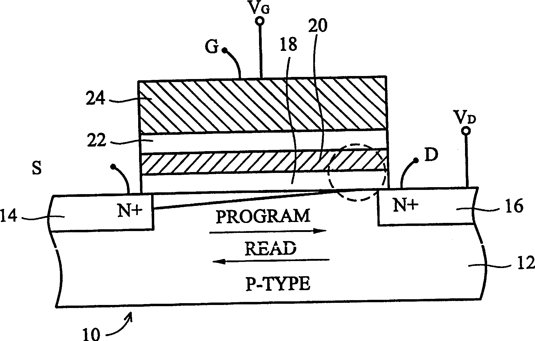
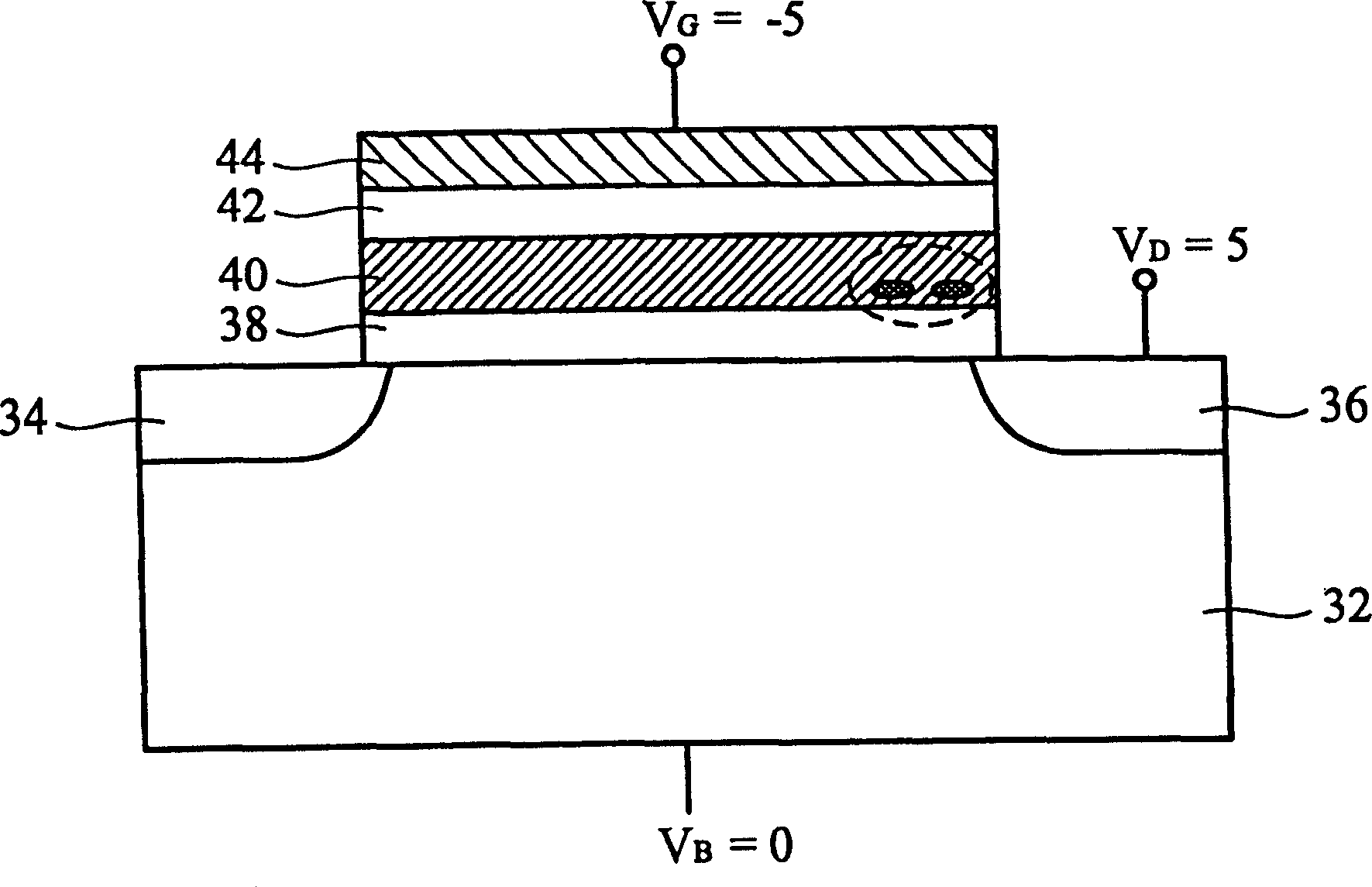
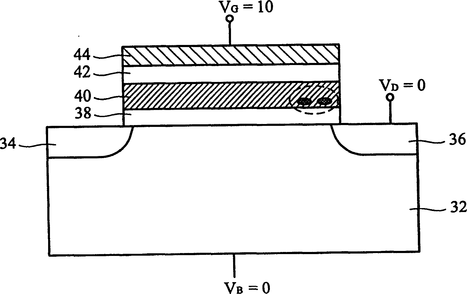
[0021] figure 2 It is a cross-sectional view of the structure of the read-only memory unit according to the embodiment of the present invention and the bias voltage applied when performing band-to-band hot hole erasing. The P-type substrate 32 has two N+ junctions separated by a channel region, one of which is a source 34 and the other is a drain 36 . Above the channel region is a silicon dioxide layer 38, which is an insulating layer, preferably with a thickness of 80-100 angstroms. Overlying the silicon dioxide layer 38 is a silicon nitride layer 40 approximately 100 Angstroms thick. The silicon nitride layer 40 is a storage storage layer capable of trapping thermal electrons injected into the silicon nitride layer 40 . Another silicon dioxide layer 42 is formed on the silicon nitride layer 40, preferably with a thickness of 80-100 angstroms. The silicon dioxide layer 42 isolates the conductive gate 44 formed on the silicon dioxide layer 42. In addition, a gate electrode ...
PUM
 Abstract
Description
Claims
Application Information