
Liquid crystal display apparatus

A liquid crystal display and equipment technology, applied in the field of liquid crystal display equipment, can solve problems such as inability to display images, degradation of display quality, increase of inductance and resistance at contacts, etc.

Inactive Publication Date: 2003-10-29
NEC LCD TECH CORP
View PDF1 Cites 3 Cited by
  • Summary
  • Abstract
  • Description
  • Claims
  • Application Information

AI Technical Summary

Problems solved by technology

In this structure, when the size of the contact used to connect the graphic symbol pixel electrode and the signal electrode is extremely fine, the inductance and resistance at the contact point increase, which may increase signal waveform distortion and voltage drop
Since the liquid crystal display device is mainly driven by alternating current, when the increased inductance and resistance cause the distortion of the signal waveform and the increase in voltage drop, the liquid crystal display device cannot even display images at a relatively low signal frequency, which leads to a decrease in display quality

Method used


Image

  • Liquid crystal display apparatus
  • Liquid crystal display apparatus
  • Liquid crystal display apparatus

Examples


no. 3 example

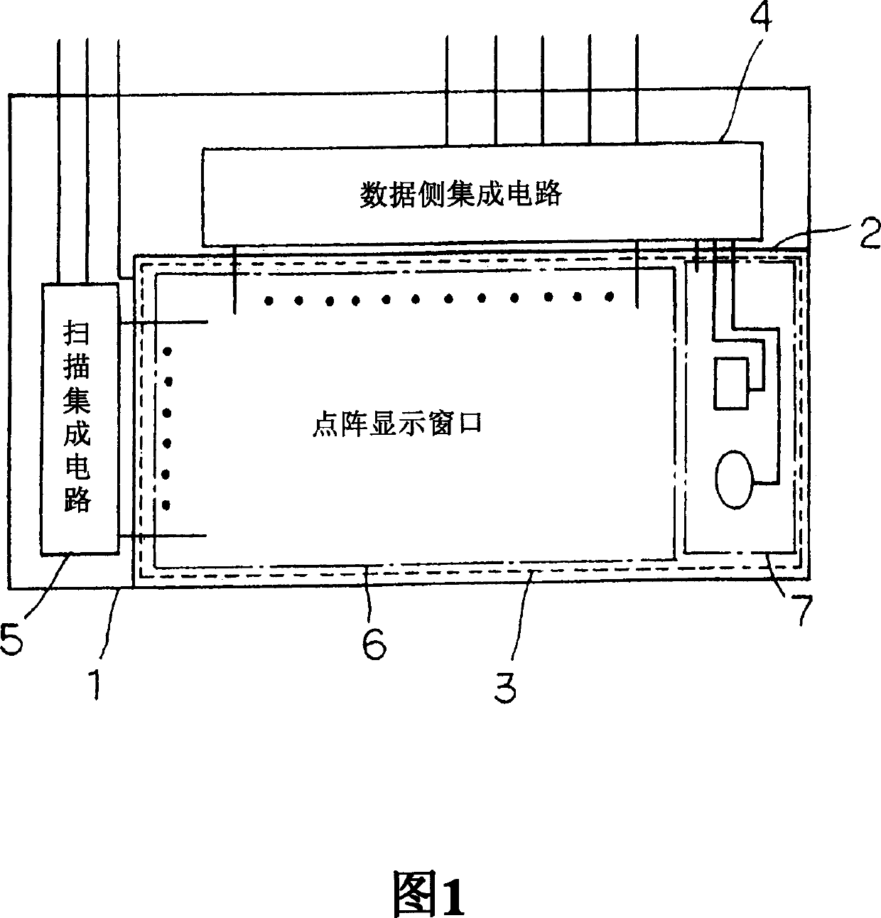
[0072] The third embodiment shows an example of a liquid crystal display device using reflective liquid crystal display elements for the dot matrix display window 6 in FIG. 1 . First, the structure of the reflective dot matrix display window 6 will be introduced with reference to FIGS. 5A and 5B.

[0073] As shown in Figure 5A, the dot matrix display window 6 in the third embodiment includes: dot matrix pixel electrodes 31, which are formed on the component substrate 1 and arranged in a grid structure; dot matrix signal electrodes 32, which straddle the insulating Layer (not shown), is formed under each dot matrix pixel electrode 31; Thin film transistor 33, it uses dot matrix signal electrode 32 as source; And contact hole 34, is used to connect dot matrix pixel electrode 31 and dot matrix signal electrode 32.

[0074] The thin film transistor 33 has a gate and a drain, the gate is connected to the scan-side integrated circuit 5 through a gate wire 35 , and the drain is conn...

no. 5 example

[0090] FIG. 7 shows a top plan view of an exemplary layout of color filters formed on a common substrate in the liquid crystal display device shown in FIG. 1 . 8 and 9 respectively show top plan views of other exemplary layouts of color filters formed on a common substrate in the liquid crystal display device shown in FIG. 1 .

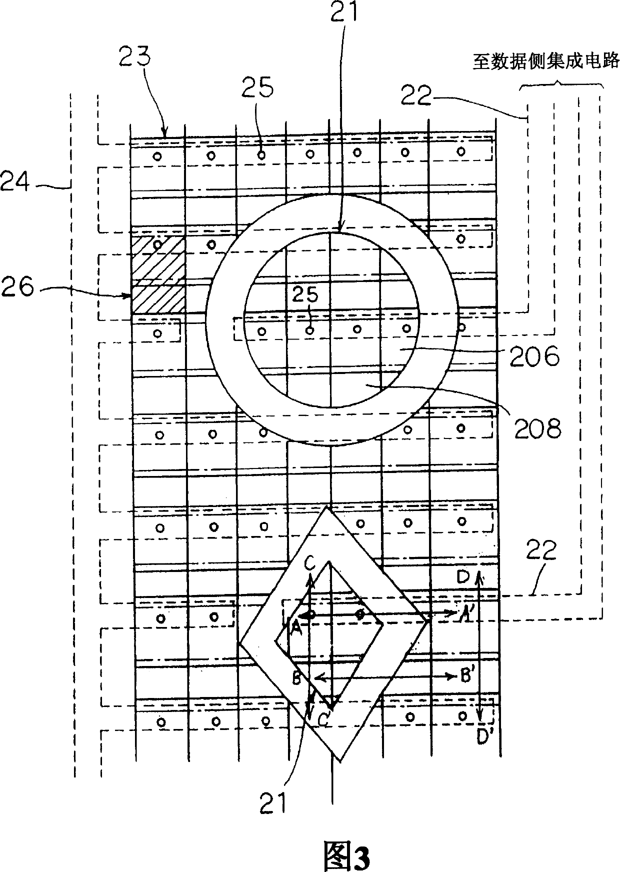
[0091] The liquid crystal display device in the fifth embodiment has R (red), G (green), B (blue) color filters formed in a stripe structure in the dot matrix display window, and the R, G, B color filters are in the The graphic symbol shows that the windows form a triangular structure. Alternatively, as shown in FIG. 8 , the R, G, and B color filters in the dot matrix display window form a strip structure, and the R, G, and B color filters in the graphic symbol display window also form a strip structure. Alternatively, as shown in FIG. 9 , the R, G, and B color filters form a mosaic structure in the graphic symbol display window.

[0092] In the fift...


PUM

PropertyMeasurementUnit
diameteraaaaaaaaaa

Abstract

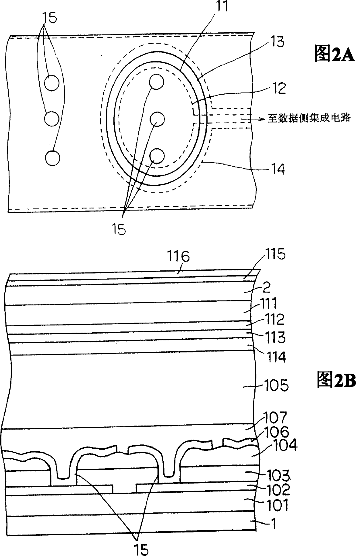
A liquid crystal display device has a first substrate, a second substrate and a liquid crystal layer. Wherein the first substrate has graphic symbol pixel electrodes for displaying graphic symbols represented by fixed patterns; the second substrate has a common electrode opposite to the graphic symbol pixel electrodes; the liquid crystal layer is sandwiched between the first substrate and the second substrate. The graphic symbol pixel electrode is formed on the interlayer insulating film, and is connected with the graphic symbol signal electrode through a plurality of contact holes, the contact holes penetrate the interlayer insulating film, and the graphic symbol signal electrode is formed under the interlayer insulating film.

Description

technical field [0001] The present invention relates to a liquid crystal display device, which has a graphic symbol display area for displaying graphic symbols, each graphic symbol represented by a fixed pattern. Background technique [0002] In portable electronic devices, such as notebook computers, mobile phones, etc., the display of graphic symbols (each symbol is represented by a fixed pattern) is becoming an indispensable function to notify the outside of changes in the status of the device (such as battery power consumption, malfunction or similar). In particular, liquid crystal display devices appearing on the market in recent years have both a dynamically driven moving image display area and a statically driven graphic symbol display area, thereby reducing cost and space. [0003] Known liquid crystal display devices are generally classified into reflective type, transmissive type, and combined reflective / transmissive type. The reflective type displays images by r...

Claims


Application Information

Patent Timeline
Patent Type & Authority Applications(China)
IPC IPC(8): G02F1/1333G02F1/1335G02F1/1343G02F1/1362G02F1/1368
CPCG02F1/134327G02F1/136227G02F1/1343
Inventor 石山敏昭渡边贵彦池田真也高桥和寿宫部光正关口金孝矢野敬和
Owner NEC LCD TECH CORP
Learn More