Semiconductor device and method for mfg. same

A semiconductor and device technology, applied in the field of manufacturing such semiconductor devices, can solve the problems of reducing mechanical reliability of packaging and defects in connection parts, etc.

Inactive Publication Date: 2003-10-29
FUJITSU LTD
View PDF2 Cites 11 Cited by
  • Summary
  • Abstract
  • Description
  • Claims
  • Application Information

AI Technical Summary

Problems solved by technology

[0006] In addition, since the interposers are connected and fixed to each other by solder balls provided in the peripheral portions of the interposers, if warpage occurs in the interposers in the stacking process of the assembly process of the semiconductor package, the interposers between the interposers Possibility of defects in connection parts
Also, when mounting a complete semiconductor package on a substrate, a defect may occur in the connection between interposers due to thermal deformation of the interposers and remelting of solder balls
[0007] In addition, since the complete semiconductor package is mechanically connected only by the solder balls over a small area, stress tends to concentrate on the connection between interposers, which may reduce the mechanical reliability of the package.

Method used


Image

  • Semiconductor device and method for mfg. same
  • Semiconductor device and method for mfg. same
  • Semiconductor device and method for mfg. same

Examples


Embodiment Construction

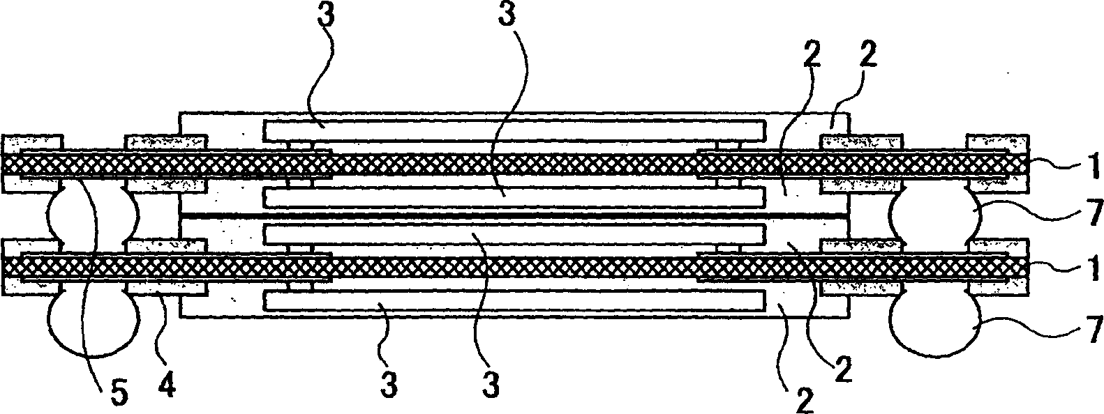
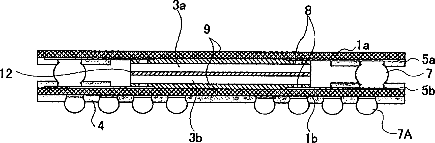
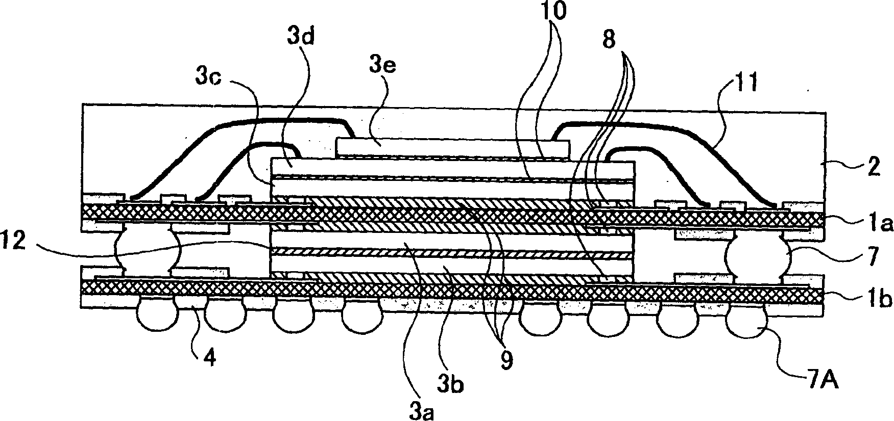
[0039] will now refer to figure 2 A semiconductor device according to a first embodiment of the present invention is described. figure 2 is a cross-sectional view of the semiconductor device according to the first embodiment of the present invention.

[0040] figure 2 The semiconductor device shown in has a structure in which an interposer 1a mounted with a semiconductor chip 3a and an interposer 1b mounted with a semiconductor chip 3b are superimposed. The interposer 1a and the interposer 1b are rearranged substrates, and are formed of polyimide tape substrates, glass epoxy resin substrates, organic substrates (polycarbonate), or the like. The interposer 1a and the interposer 1b are connected to each other by solder balls 7 as conductive members.

[0041] The semiconductor chip 3a is mounted on the interposer 1a by a flip-chip mounting method generally called face-down mounting. That is, the semiconductor chip 3 a is electrically connected to electrode blocks formed on...


PUM


Abstract

A stacked type semiconductor device has a reduced overall height and reliability of improving the mechanical strength of the stacked structure. The semiconductor device also has improved heat dissipation characteristics. The first interposer has a surface on which the first electrode pads are formed, and the first semiconductor element is mounted such that the circuit forming surface is opposed to the first interposer. The second semiconductor element has a circuit forming surface and a back surface opposite to the circuit forming surface. The second interposer has a surface on which second electrode pads are formed, and the second semiconductor element is mounted such that the circuit forming surface is opposed to the second interposer. External connection terminals are provided on the surface of the second interposer opposite to the surface on which the second semiconductor element is mounted. The first and second inserts are electrically connected to each other by the conductive member therebetween. The back surface of the first semiconductor element and the back surface of the second semiconductor element are fixed to each other by an adhesive.

Description

technical field [0001] The present invention generally relates to semiconductor devices, and more particularly to a semiconductor device having a three-dimensional structure in which a plurality of semiconductor devices and semiconductor elements are stacked, and a method for manufacturing the semiconductor device. [0002] With the recent development of electronic equipment, there is an increasing demand for semiconductor devices that are reduced in size and thickness, multifunctional, high performance, and high density. In order to meet this demand, the structure of semiconductor devices has shifted to a three-dimensional structure in which a plurality of semiconductor devices or a plurality of semiconductor elements are stacked. Background technique [0003] Japanese Patent Laid-Open No. 2001-223297 discloses a semiconductor device having a three-dimensional structure formed by stacking a plurality of semiconductor devices. figure 1 is a cross-sectional view of the semic...

Claims


Application Information

Patent Timeline
Patent Type & Authority Applications(China)
IPC IPC(8): H01L25/18H01L25/065H01L25/07H01L25/10H01L25/11
CPCH01L25/03H01L25/0657H01L25/105H01L2224/16H01L2224/32145H01L2224/32225H01L2224/48091H01L2224/48227H01L2224/73204H01L2224/73253H01L2224/73265H01L2225/0651H01L2225/06513H01L2225/06517H01L2225/0652H01L2225/06541H01L2225/06558H01L2225/06572H01L2924/01079H01L2924/15311H01L2924/15331H01L2225/1023H01L2225/1058H01L2225/1094H01L2224/16225H01L2924/3511H01L2224/45144H01L24/73H01L2924/00014H01L2924/00012H01L2924/00011H01L2924/00H01L23/48
Inventor 西村隆雄宇野正小野寺浩高岛晃
Owner FUJITSU LTD
Why Eureka
Try Eureka