Semiconductor device and producing method thereof

A technology of electronic devices and electronic components, applied in the direction of semiconductor devices, semiconductor/solid-state device components, electric solid-state devices, etc., to achieve the effects of enhancing heat radiation characteristics, shortening the distance, and preventing temperature rise

Inactive Publication Date: 2003-11-05
NEC COMPOUND SEMICON DEVICES
View PDF7 Cites 18 Cited by
  • Summary
  • Abstract
  • Description
  • Claims
  • Application Information

AI Technical Summary

Problems solved by technology

Therefore, a semiconductor device including a multi-chip module cannot avoid the extra weight derived from the space 127

Method used


Image

  • Semiconductor device and producing method thereof
  • Semiconductor device and producing method thereof
  • Semiconductor device and producing method thereof

Examples


no. 2 example

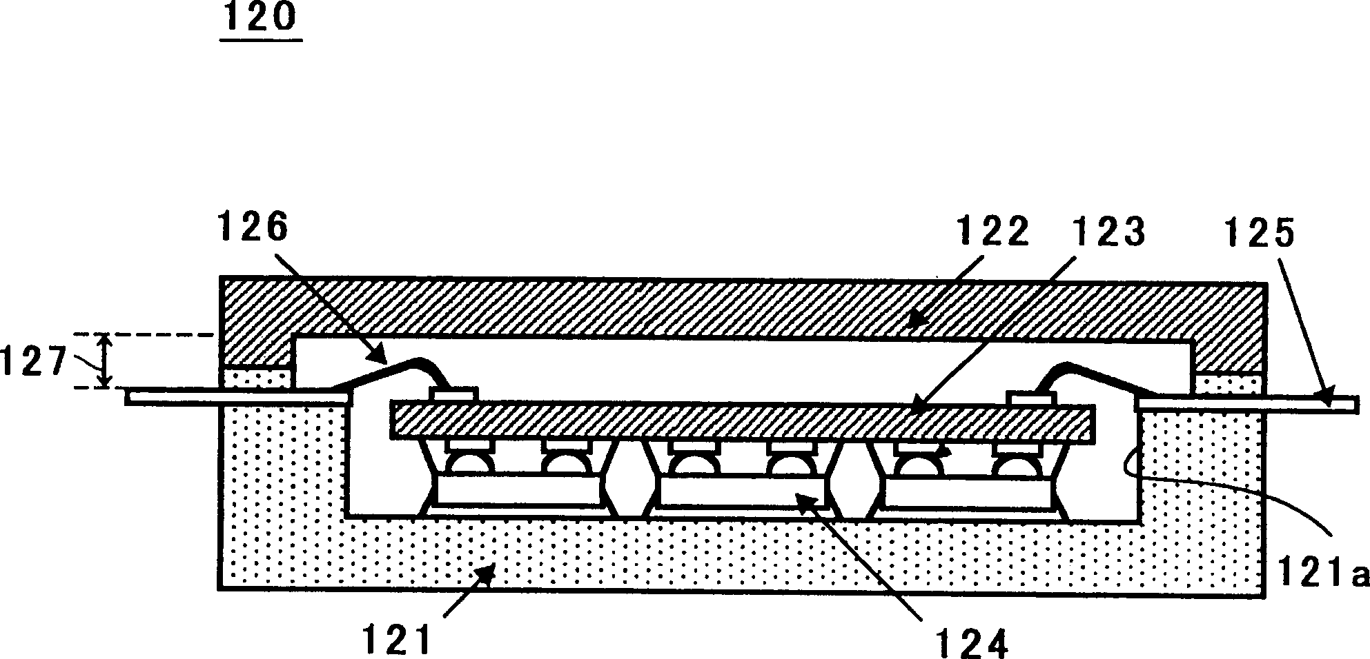
[0082] Figure 5 is a cross-sectional view of the electronic device 20 according to the second embodiment.

[0083] In the electronic device 10 according to the first embodiment, the high-frequency IC 14 is electrically connected to the electrode 12c through the bonding wire 17. In contrast, in the second embodiment, the high frequency IC 14 is electrically connected to the cover type wiring substrate 12 in a contact chip connection manner.

[0084] The structure of the electronic device 20 according to the second embodiment is the same as that of the electronic device 10 according to the first embodiment except that the high-frequency IC 14 is electrically connected to the cover type wiring substrate 12 by contact chip connection.

[0085] In the electronic device 20, on the upper surface of the high-frequency IC 14, it is electrically connected to the cover type wiring substrate 12 in the form of a contact chip. Thus, if Figure 5 As shown, the high frequency IC 14 can be...

no. 1 example

[0095] Similar to the first embodiment, by directly coupling the lead frame 11 and the cover type wiring substrate 12 together, the length of the wire can be shortened as a result.

[0096] Such as image 3 As shown, in the electronic device 10 according to the first embodiment, the high-frequency IC 14 is electrically connected to the cover type wiring substrate 12 through the bonding wire 17 . In contrast, in the electronic device 20 according to the second embodiment, the high frequency IC 14 is electrically connected to the cover type wiring substrate 12 in a contact chip connection manner. Therefore, compared with the electronic device 10 according to the first embodiment, it is possible to further shorten the length of the wire, and suppress delay of signals and electromagnetic noise, both of which are proportional to the length of the wire.

[0097] A fifth advantage is that it is possible to enhance the heat radiation characteristics of the electronic device 20 .

[0...

no. 3 example

[0100] Image 6 is a cross-sectional view of the electronic device 30 according to the third embodiment.

[0101] In the electronic device 30 according to the third embodiment, three high-frequency ICs 14 are mounted on a cover type wiring substrate 12, and a lead frame 11 is formed on one surface on which three high-frequency ICs 14 are arranged, etc. Three grooves 15 are formed. Each groove 15 is associated with a high frequency IC 14 .

[0102] The electronic device 30 according to the third embodiment has the same structure as the electronic device 20 according to the second embodiment except that the electronic device 30 includes three high-frequency ICs 14 and three grooves 15 .

[0103] In addition to including the steps of simultaneously coupling three high-frequency ICs 14 with the covering type wiring substrate 12 in the form of contact chips in the method of manufacturing the electronic device 30, and simultaneously generating three depressions on the surface of t...


PUM


Abstract

An electronic device (10) comprising: (a) a first wiring substrate (11) comprising a metal region (111) formed with a groove (15) extending to the metal region (111); and (b) The second wiring substrate (12) includes a ground electrode. When connected to the first wiring substrate (11), the grounding electrode is formed in the groove (15) and the area outside the signal transmission channel around the groove (15). pole; further comprising at least one first electronic component (14) mounted thereon. The first and second wiring substrates (11, 12) are directly coupled to each other such that the first electronic component (14) is placed within the recess (15).

Description

technical field [0001] The present invention relates to an electronic device including an electronic component and a manufacturing method thereof, in particular to a semiconductor device and a manufacturing method thereof. Background technique [0002] In order to meet the demand for higher integration and higher operating speed in recent LSIs, it is recommended to use a large number of chips, which include a plurality of pins and operate at a clock frequency of 100 MHz or higher. In devices including such chips operating at high speeds, there is a significant delay in the signal transmission through the interposer and the printed board, and the parasitic capacitance and inductance of the interposer cannot be ignored. Such signal delays and parasitic capacitances prevent the entire system including this device from operating at high speeds. [0003] To solve these problems, a multi-chip module (MCM) is proposed. A multi-chip module includes multiple chips, which are arrang...

Claims


Application Information

Patent Timeline
Patent Type & Authority Applications(China)
IPC IPC(8): H01L23/12H01L23/31H01L23/495H01L23/66
CPCH01L23/3107H01L23/49503H01L23/49531H01L23/66H01L2224/16H01L2224/48091H01L2224/48247H01L2224/73253H01L2924/15153H01L2924/15165H01L2924/16152H01L2924/19041H01L2924/19105H01L2924/30107H01L2924/3025H01L24/48H01L2224/05599H01L2224/45099H01L2224/85399H01L2924/00014H01L2924/14H01L24/49H01L2224/49175H01L2224/45015H01L2924/207H01L2924/00H01L23/48
Inventor 中泽大望平沢宏希
Owner NEC COMPOUND SEMICON DEVICES
Why Eureka
Try Eureka