

Semiconductor memory device with data bus scheme for reducing high frequency noise
一种数据总线、存储器的技术,应用在半导体存储器领域,达到简化工艺、提高电压裕度、减少成本的效果
- Summary
- Abstract
- Description
- Claims
- Application Information
AI Technical Summary
Problems solved by technology
Method used
Image

Examples
Embodiment Construction
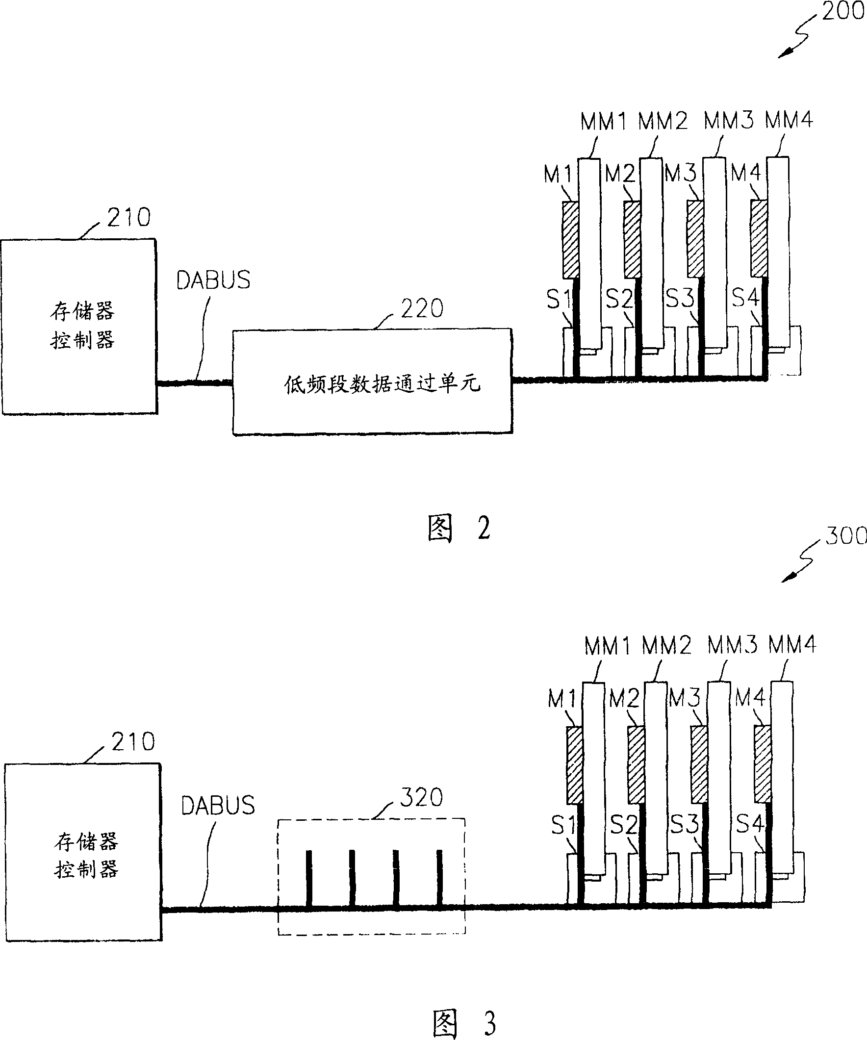
[0037] FIG. 2 is a schematic diagram of a semiconductor memory according to a first preferred embodiment.
[0038] Referring to FIG. 2, a semiconductor memory 200 according to a first preferred embodiment includes a plurality of memory modules MM1 to MM4 and a data bus (DABUS), the plurality of memory modules having memories M1 to M4 respectively, which transmits data to Memory modules MM1 to MM4. The data bus (DABUS) includes a low frequency band data pass unit (low frequency band data pass unit) 220, which removes high frequency components higher than a specific "cut-off" frequency in the data, and converts the filtered data Transfer to memory modules MM1 to MM4.
[0039] Referring now to FIG. 2, the working principle of the semiconductor memory according to the first preferred embodiment will be described in detail.
[0040] 2 shows a memory controller 210 for controlling the memories M1 to M4, and memory modules MM1 to MM4 respectively having the memories M1 to M4, and s...
PUM
 Abstract
Description
Claims
Application Information