Method and apparatus for adaptive compensation of dead time for inverter and converter

A dead time, inverter technology, applied in the output power conversion device, the conversion of AC power input to DC power output, electrical components and other directions, can solve problems such as difficulty in reducing Uuo

Inactive Publication Date: 2004-01-14
DELTA ELECTRONICS INC
View PDF0 Cites 9 Cited by
  • Summary
  • Abstract
  • Description
  • Claims
  • Application Information

AI Technical Summary

Problems solved by technology

However, for smaller positive currents, during the dead time, due to the larger off-time T off and the parasitic inductance and capacitance of the system so that U uo Difficult to lower
Therefore the high voltage U uo Decays slowly during dead time

Method used


Image

  • Method and apparatus for adaptive compensation of dead time for inverter and converter
  • Method and apparatus for adaptive compensation of dead time for inverter and converter
  • Method and apparatus for adaptive compensation of dead time for inverter and converter

Examples


Embodiment Construction

[0046] Although the present invention can be implemented in various forms, in order to simplify the description, the details of some preferred embodiments will be further described and illustrated below. However, the content disclosed here is to illustrate the principle of the present invention, but not limited to the following embodiments.

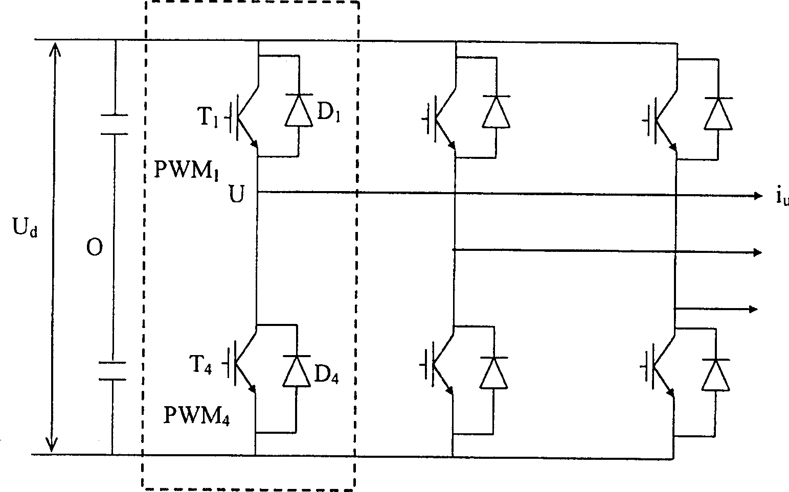
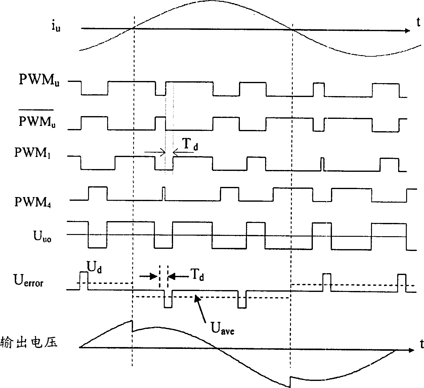
[0047] As mentioned above, the voltage shift caused by the dead time is in the opposite direction to the output current, and its magnitude depends on the direction of the output current. For simplicity, the voltage offset waveform is simplified as Figure 7 The trapezoid shown. see Figure 7 , at t 2 with t 3 During, because the delay time is large enough to automatically compensate the dead time, and at t 1 with t 2 period and t 3 with t 4 During this period, the delay time is gradually increased, and the dead time part is automatically compensated. To compensate for this offset voltage, as Figure 7 The reverse voltage shown i...


PUM


Abstract

The invention relates to the compensation of dead time effect in electronic appliances such as inverters or converters having one or more legs with two complementary switches. The invented method mainly includes following steps providing an initial pulse width modulated (PWM) reference, providing a bias current and detecting the bias current crossing points, providing a dead time compensation signal which is adjusted responsive to the crossing points, and adding the dead time compensation signal to the PWM reference. Hence an adaptive compensation is accomplished independent of types of switching elements and load conditions. A high reliable circuit with low cost is further included as a preferred embodiment of bias current crossing points detection.

Description

(1) Technical field [0001] The present invention relates to a device and method for compensating the voltage error generated by the dead time effect of the switching element when applied to the control of a converter (converter), an inverter (inverter) or a motor, especially an application A device and method for compensating voltage errors and output current distortions generated by dead time effects of switching elements in PWM converters or PWM inverters. (2) Background technology [0002] see figure 1 , figure 1 It is a schematic diagram of an inverter circuit composed of semiconductor switching elements. Wherein, the inverter is formed by a phase bridge, and the phase bridge is formed by a pair of switching elements connected in parallel with reverse recovery diodes connected in series. A load is connected to a node of the series-connected switching elements, and the node is defined as an output end of the inverter. [0003] As we all know, when a typical semiconduc...

Claims


Application Information

Patent Timeline
Patent Type & Authority Applications(China)
IPC IPC(8): H02M7/5387
CPCH02M2001/385H02M2001/0009H02M7/5387H02M1/0009H02M1/385
Inventor 应建平吴志敢王进
Owner DELTA ELECTRONICS INC
Why Eureka
Try Eureka