Differential high speed cmos to ecl logic converter

A converter and differential technology, applied in the direction of logic circuit interface device, logic circuit connection/interface layout, pulse generation, etc., can solve the problem of no differential output, etc., and achieve the effect of low operating voltage

Inactive Publication Date: 2004-01-14
ALCATEL LUCENT SAS
View PDF4 Cites 6 Cited by
  • Summary
  • Abstract
  • Description
  • Claims
  • Application Information

AI Technical Summary

Problems solved by technology

Goodell circuit is asymmetric and has no differential output

Method used


Image

  • Differential high speed cmos to ecl logic converter
  • Differential high speed cmos to ecl logic converter
  • Differential high speed cmos to ecl logic converter

Examples


Embodiment Construction

[0039] Those skilled in the art will realize that the following description of the invention is illustrative only and not limiting in any way. Other embodiments of the present invention will be readily apparent to those skilled in the art upon reading this specification.

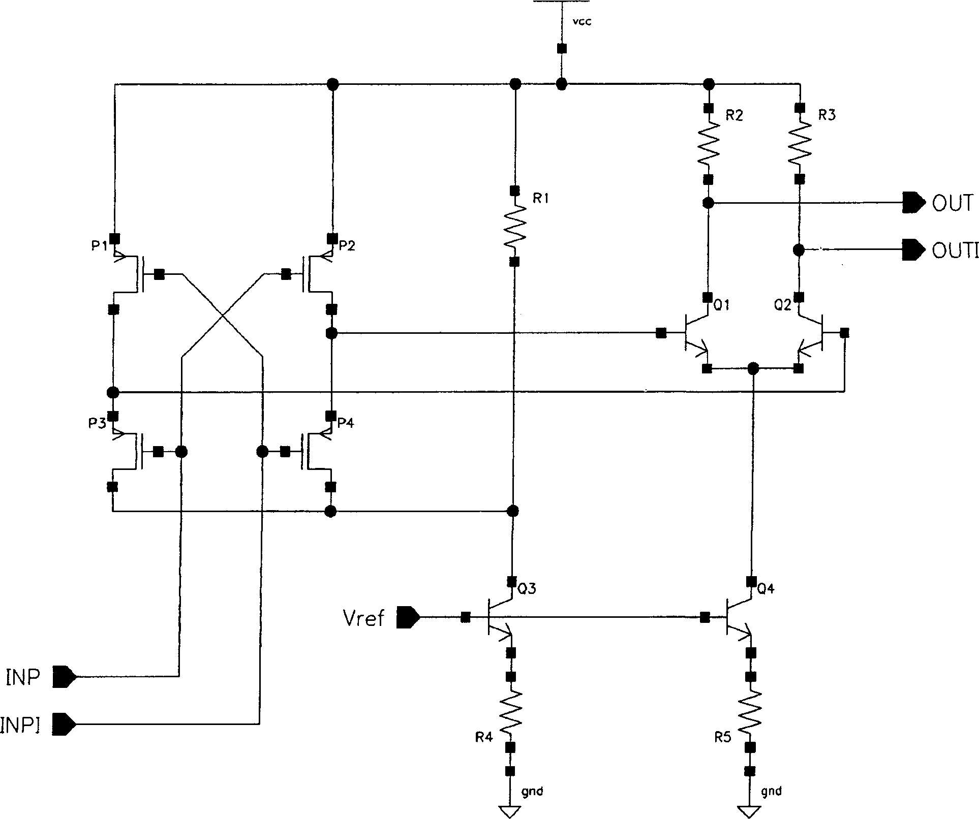
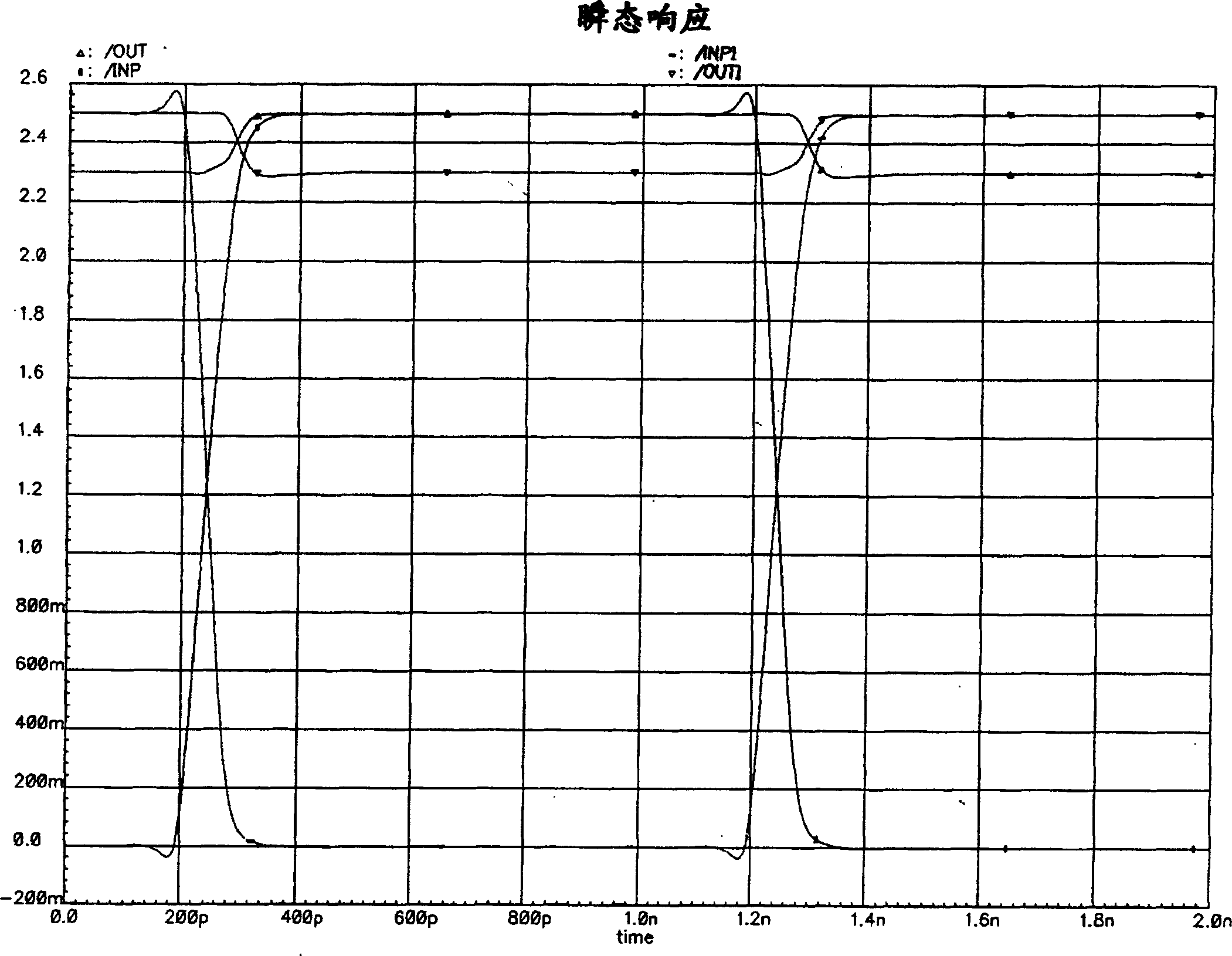
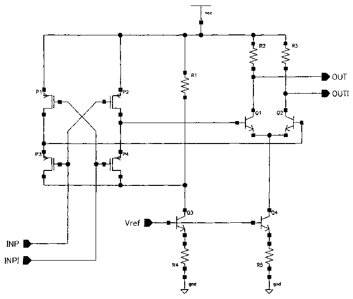
[0040] figure 1 The high speed, low hysteresis logic level translator of the present invention is shown in simplified form. The converter is used to convert a differential complementary pair of input signals at input nodes INP and INPI (input and inverting input) from potentials associated with CMOS logic levels to output nodes OUT and OUTI at potentials associated with ECL logic levels The output signal is a differential complementary pair. It is contemplated that the potentials associated with OUT and OUTI may be generated by converters at levels other than those associated with ECL, including but not limited to firing transceiver logic (GTL).

[0041] The converter of the present invention comprises tw...


PUM


Abstract

A logic level converter for translating differential CMOS logic signals to into differential logic signal pairs such as those associated with ECL levels. The converter includes two components. A first component consists of two branches coupled to the switchable CMOS level input and it provides a first switchable translated output. The second component is an ECL current switch. The current associated with the converter is mirrored through the branches to minimize the effects of fabrication, temperature, and / or power supply vagaries, as well as a very fast and tolerance independent signal level translation.

Description

field of invention [0001] The present invention relates to circuits for transmitting electrical signals from one location to another. In particular, the present invention relates to a converter for changing logic levels associated with operation of complementary metal oxide silicon (CMOS) transistors to logic levels associated with operation of emitter coupled logic (ECL) transistors. The present invention is based on priority application No. EP 02 360 180.0, which is hereby incorporated by reference. Background technique [0002] Voltage level translators are used to adjust the logic high and logic low voltage levels associated with a single input signal or pair of input signals into the converter to high and low voltage levels compatible with downstream circuitry. The converter must transmit these electrical signals at the desired amplitude and rate. Signal transmission between active devices on the same semiconductor-based chip or on different chips. Devices may be adj...

Claims


Application Information

Patent Timeline
IPC IPC(8): H03K19/0175
CPCH03K19/017527
Inventor 弗兰克·爱尔切曼
Owner ALCATEL LUCENT SAS
Why Eureka
Try Eureka