Full optical packet switching node structure for supporting burst or non-burst businesses
A technology of optical packet switching and node structure, applied in the field of optical communication, can solve problems such as uneconomical and effective, and achieve the effects of large buffer capacity, reduced volume and cost, and reduced number of wavelength converters
- Summary
- Abstract
- Description
- Claims
- Application Information
AI Technical Summary
Problems solved by technology
Method used
Image
Examples
Embodiment Construction
[0027] The specific implementation of the technical solution of the present invention will be described in detail below in conjunction with the accompanying drawings.
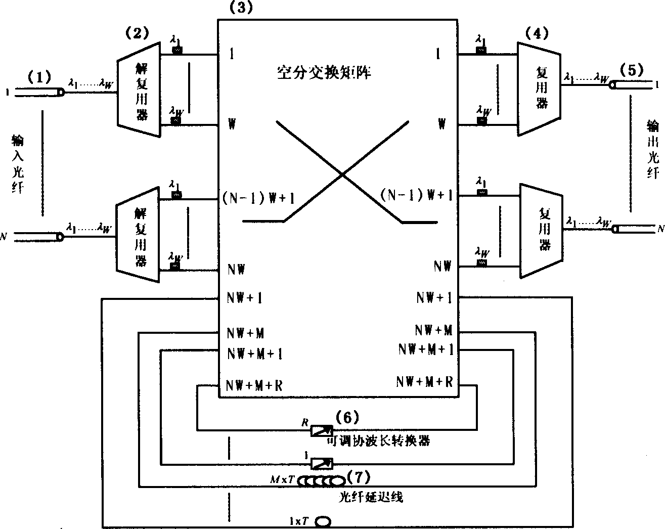
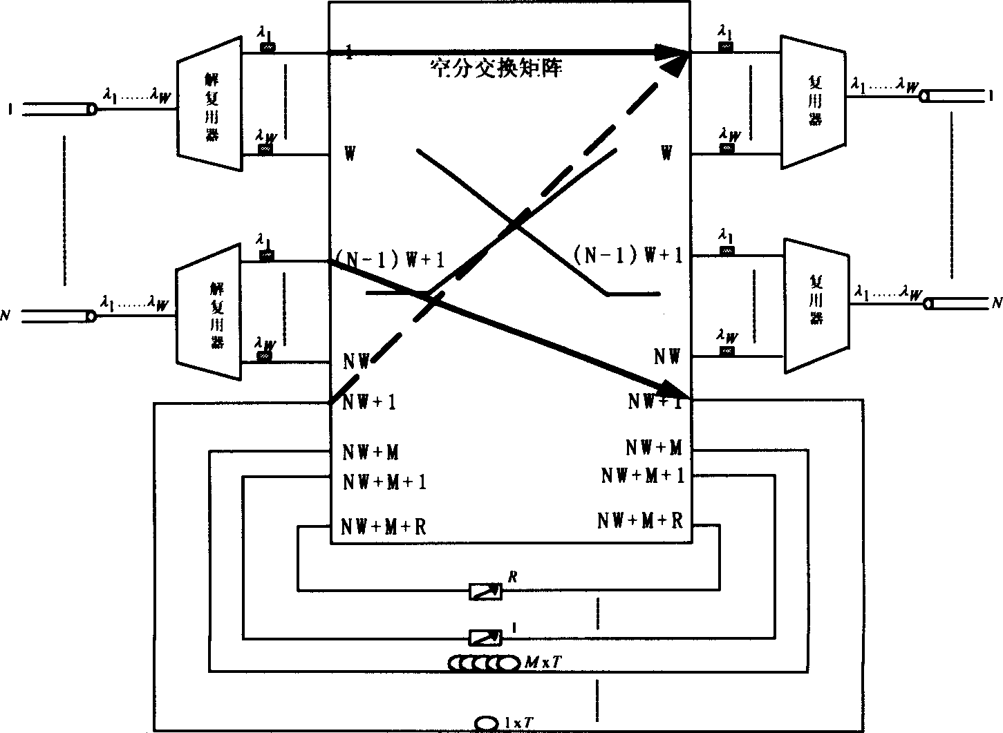
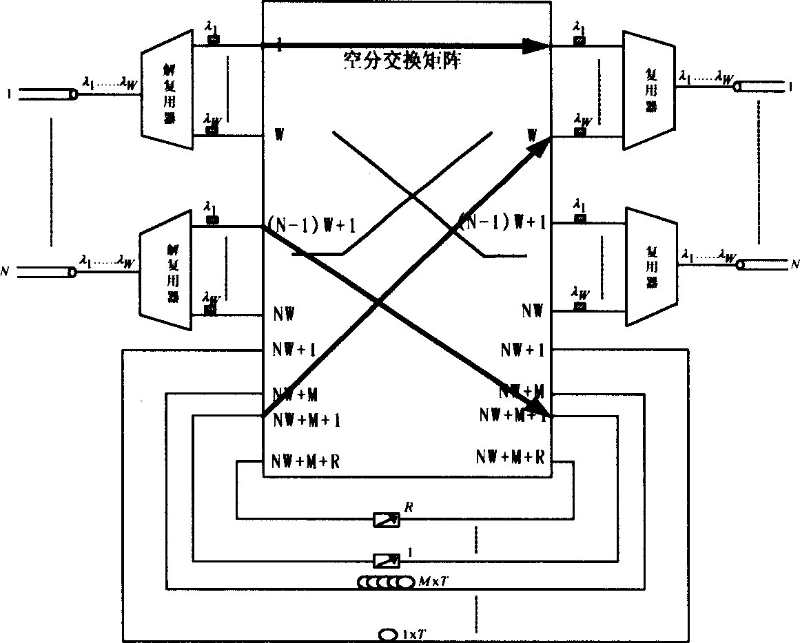
[0028] figure 1 It is a schematic diagram of the switching node structure of the present invention. If the switching structure of the present invention supports N input fiber ports and N output fiber ports, each fiber can support W wavelength channels, denoted as {λ 1 ,...λ w}, then the whole switching structure of the present invention consists of N 1×W optical wavelength division multiplexers, N W×1 optical wavelength division multiplexers, and one (WN+R+M)×(WN+R+M) non-blocking An optical switch matrix, R tunable full-wavelength converters, and M optical fiber delay lines. Among them, M fiber delay lines form a degenerate structure, that is, the delay time length of the M fiber delay lines changes continuously, and the step size is T, where T is the duration of a time slot. The delay line with the shortes...
PUM
 Abstract
Description
Claims
Application Information


