Organic electrofluorescence device and producing mehtod thereof

An electroluminescent device and organic technology, which is applied to electroluminescent light sources, electric light sources, electrical components, etc., can solve the problem of not being able to ensure the uniformity of the organic functional layer evaporation at the same time. The metal layer is complete, the isolation effect is poor, and the pixel points are short-circuited. and other problems, to achieve the effect of improving life and luminous uniformity, improving life, and reducing the number of processes.

Inactive Publication Date: 2004-02-04
TSINGHUA UNIV +1
View PDF2 Cites 17 Cited by
  • Summary
  • Abstract
  • Description
  • Claims
  • Application Information

AI Technical Summary

Problems solved by technology

[0004] ① The baking temperature of the photoresist (such as 120°C) will damage the organic film;
[0005] ② Solvents, developers, and corrosive solutions of photoresist will damage the organic film;
[0012] Make the pixel short-circuit and not emit light;
[0013] (2) The single-layer spacer column 4 can only be distributed parallel to the direction perpendicular to the transparent electrode 2, and se...

Method used


Image

  • Organic electrofluorescence device and producing mehtod thereof
  • Organic electrofluorescence device and producing mehtod thereof
  • Organic electrofluorescence device and producing mehtod thereof

Examples


Embodiment 1

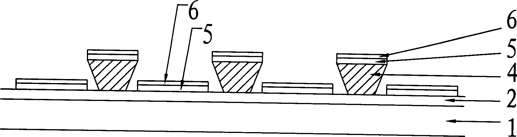
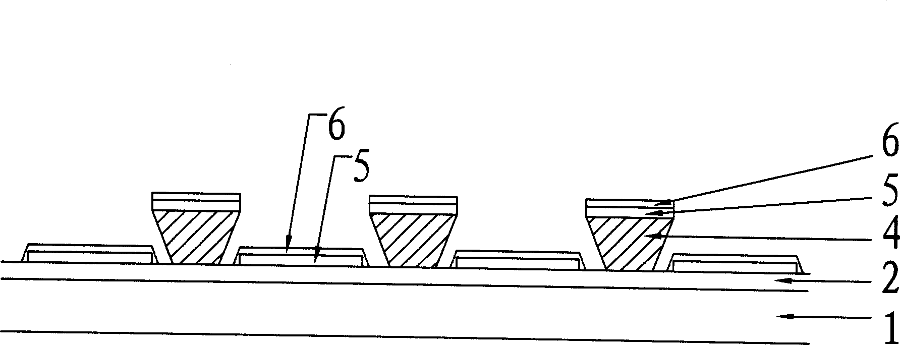
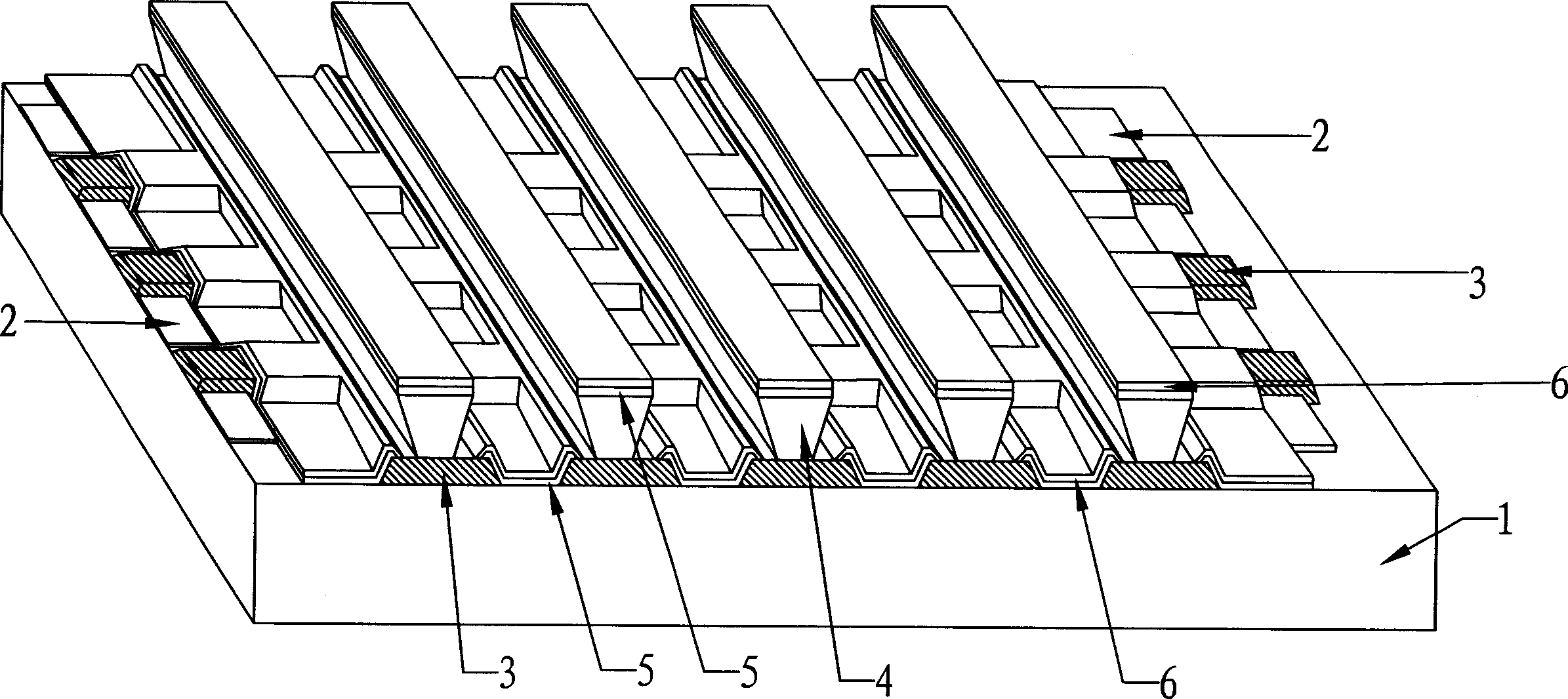
[0141] (The entire preparation process of OLED is carried out in the purification workshop.) Use UV and lotion containing surfactant to clean and dry the ITO glass with a square resistance of 15Ω. The film thickness of ITO is 170nm. A group of parallel and separated straight lines with a line width of 400 μm and a line gap of 30 μm. Wash and dry again, and then spin-coat the first layer of organic insulating material photosensitive PI DL-1000 with a film thickness of 1.5 μm, and bake in a convection oven at 125°C for 25 minutes. The first layer is exposed but not developed, and the exposure pattern is a network structure, that is, only the light-emitting area and the lead connection area of ​​the pixel point of the device are exposed. The width of the line parallel to the ITO line is 45 μm, and the line perpendicular to the ITO line The width is 40 μm. Then continue to spin-coat the second layer of insulating material negative photoresist ZPN1168-30 on the first organic insul...

Embodiment 2

[0142] (The entire preparation process of OLED is carried out in the purification workshop.) Use UV and lotion containing surfactant to clean and dry the ITO glass with a square resistance of 5Ω. The ITO film thickness is 200nm. A group of parallel and separated straight lines with a line width of 200 μm and a line gap of 20 μm. Wash and dry again, and then spin-coat the first layer of organic insulating material photosensitive PI DL-1000 with a film thickness of 1.2 μm, and bake in a convection oven at 125°C for 25 minutes. Immediately continue to spin-coat the second layer of organic insulating material negative photoresist Tlor-n on the first organic insulating layer with a film thickness of 4 μm, and bake in a hot plate at 110° C. for 90 s. Then the second layer is exposed, the exposure pattern is a group of parallel and separated straight lines perpendicular to the ITO lines, the line width is 15 μm, and baked in a hot plate at 110°C for 60s. Use 2.38% TMAHO solution to ...


PUM


Abstract

The invention relates to an organic electro-luminescence device and the manufacturing method thereof in the technical field of electronic and semiconductor component. A double-layer insulating column is provided for on the pattern of the first electrode (2) of the device, the cross section of the line of the second layer (8) of the insulating column has the shape that its width is decreased from up to down, and its hypotenuse has two sequentially convergent angles alpha,beta, and alpha>beta. Then the organic functioning layer (5) and the second electrode (6) are deposited sequentially. The angle beta of the hypotenuse of the second layer (8) of the insulating column can increase greatly the tolerance of the evaporating angle and the evaporating thickness of the metal back electrode, and the organic functioning layer can be fully covered by the metal back electrode by using the different evaporating angles between the organic functioning layer and the metal back electrode.

Description

technical field [0001] The invention relates to an organic electroluminescence device and a preparation method of the device, belonging to the technical field of electronic semiconductor components. Background technique [0002] Organic Electroluminescent Devices (Organic Electroluminescent Devices, hereinafter referred to as OLEDs) are generally composed of a transparent first electrode located on a transparent substrate, an organic electroluminescent medium (organic functional layer) deposited on the first electrode, and an organic electroluminescent medium (organic functional layer) located on the transparent substrate. The second electrode (metal electrode) above the organic electroluminescence medium. The transparent electrode serves as the anode of the device, and the metal electrode serves as the cathode of the device. Apply a high level to the transparent electrode and a low level to the metal electrode to make the device emit light. A group of anodes (or cathodes)...

Claims


Application Information

Patent Timeline
IPC IPC(8): H05B33/10H05B33/12
Inventor 邵玉暄邱勇
Owner TSINGHUA UNIV
Why Eureka
Try Eureka