Preparation method of ZnAl*0*/alpha-Al*0*composite base material

A composite substrate and mixed material technology, which is used in semiconductor/solid-state device manufacturing, semiconductor devices, electrical components, etc., can solve the problems of complex process, high lattice mismatch, high dislocation density, etc., and achieves simple process and high quality. Stable and easy-to-operate effect

Inactive Publication Date: 2004-02-18
SHANGHAI INST OF OPTICS & FINE MECHANICS CHINESE ACAD OF SCI
View PDF0 Cites 7 Cited by
  • Summary
  • Abstract
  • Description
  • Claims
  • Application Information

AI Technical Summary

Problems solved by technology

[0005] Prior α-Al 2 o 3 Substrate and pulsed laser deposition (PLD: pulsed laser deposition) technology to prepare ZnAl 2 o 4 / α-Al 2 o 3 The significant disadvantages of the composite substrate are: (1) the use of α-Al 2 o 3 As substrate, α-Al 2 o 3 The lattice mismatch between GaN and GaN is as high as 14%, so that the prepared GaN film has a high dislocation density and a large number of point defects; (2) the pulse laser deposition technology uses the prior α-Al 2 o 3 Prepare ZnO film on the surface of the substrate, and then prepare ZnAl 2 o 4 Two-step process of covering layer, complicated process and unstable quality

Method used


Image

  • Preparation method of ZnAl*0*/alpha-Al*0*composite base material
  • Preparation method of ZnAl*0*/alpha-Al*0*composite base material

Examples


Embodiment Construction

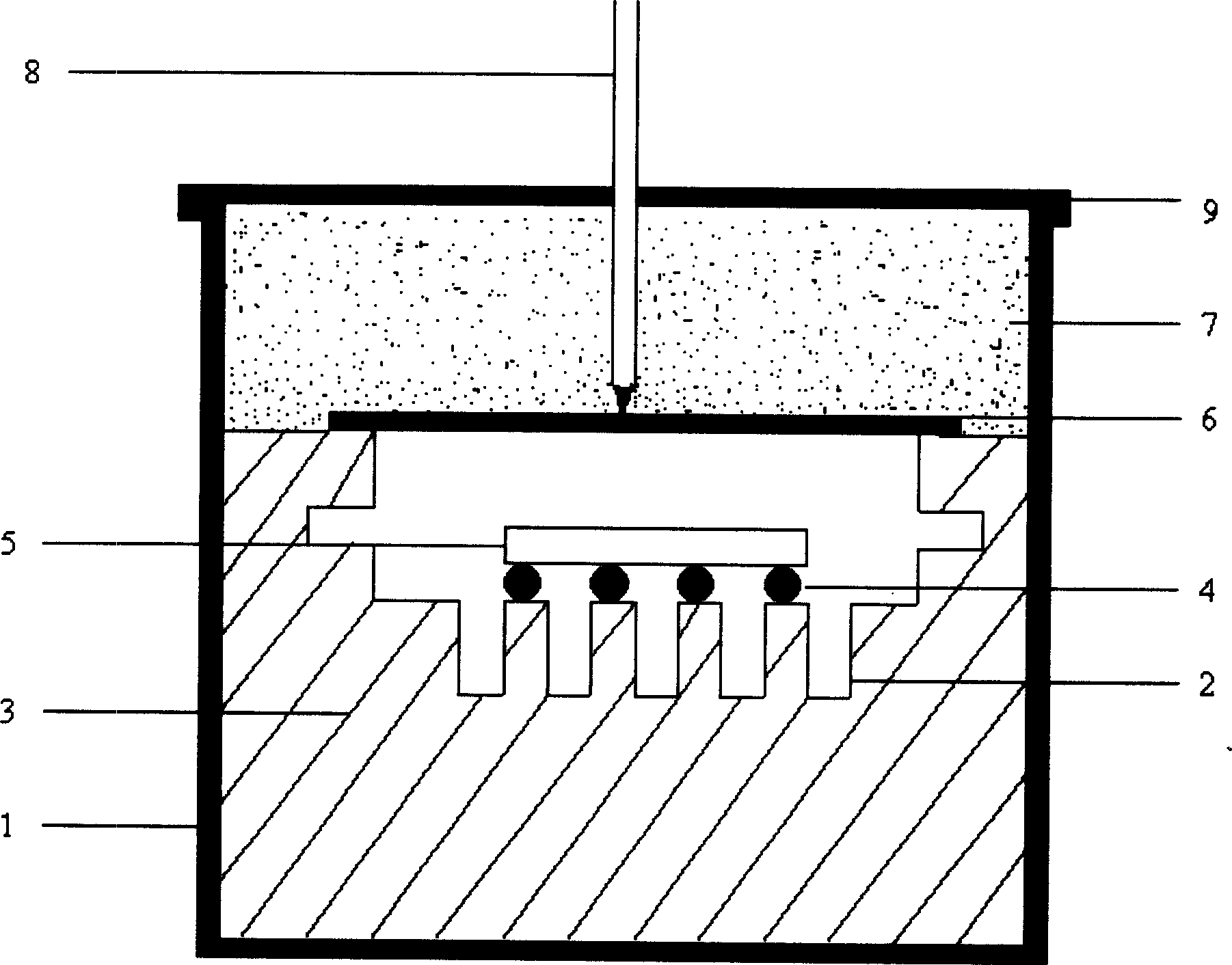
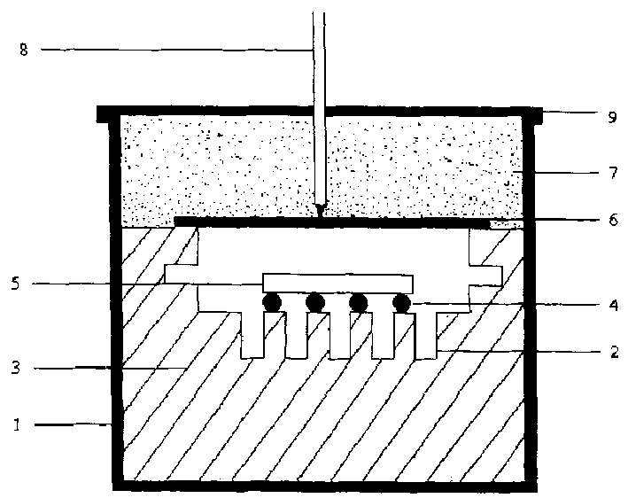
[0017] see first figure 1 , the gas phase transport equilibrium (VTE) technology used in the present invention prepares composite substrate material ZnAl 2 o 4 / α-Al 2 o 3 For a schematic diagram of the device, see figure 1 , in the platinum crucible 1, a certain ratio of ZnAl with pores 2 is placed 2 o 4 Mix block 3 with ZnO, the upper part of block 3 is platinum wire 4, sapphire α-Al polished on both sides or single side 2 o 3 The wafer 5 is placed on the platinum wire 4, and the upper part of the material block 3 has a platinum sheet 6 and ZnAl 2 o 4 Cover with powder 7 mixed with ZnO, insert thermocouple 8 into powder 7, and add platinum cover 9 to the top of crucible 1 to seal.

[0018] Vapor Transport Equilibrium (VTE) technology is a mass transfer process, so there should be sufficient supply of ZnO in the crucible, and secondly, the balance of the gas phase depends on the continuous transfer of ZnO from ZnAl to ZnO. 2 o 4 To maintain the volatilization in th...


PUM


Abstract

The method includes the following steps: placing ZnAl2O4 and ZnO mixed material block with gas holes into platinum crucible, placing or hanging either double face polished or single face polished sapphire a-Al2O3 wafer on platinum filament, setting crucible cover blanketed with ZnAl2O4 and ZnO mixed power and thermocouple and setting platinum cover on crucible top for seal, placing it into resistance furnace, heating the furnace temperature up to 1000-1400 deg., keeping it constant for 20-100 hour to let ZnO diffuse into a-Al2O3 uafer and decreasing temperature to obtain ZnA2O4 / a-Al2O3 compound substrate material.

Description

technical field [0001] The present invention relates to a kind of ZnAl 2 o 4 / α-Al 2 o 3 Preparation method of composite substrate material. ZnAl 2 o 4 / α-Al 2 o 3 The composite substrate material is mainly used for the epitaxial growth of InN-GaN-based blue light semiconductor. Background technique [0002] Group III nitride semiconductor material InN-GaN has excellent characteristics, such as stable physical and chemical properties, high thermal conductivity and high electron saturation velocity, and the optical transition probability of direct bandgap materials is an order of magnitude higher than that of indirect bandgap materials. Therefore, broadband Gap InN-GaN-based semiconductors show promising applications in short-wavelength light-emitting diodes, lasers, and UV detectors, as well as high-temperature electronic devices. Due to the relatively high melting point of InN-GaN, N 2 The saturated vapor pressure is high, and the preparation of InN-GaN bulk singl...

Claims


Application Information

Patent Timeline
IPC IPC(8): H01L21/00H01L33/00H01L33/02
Inventor 徐军王海丽周圣明杨卫桥彭观良周国清宋词杭寅蒋成勇司继良赵广军
Owner SHANGHAI INST OF OPTICS & FINE MECHANICS CHINESE ACAD OF SCI
Why Eureka
Try Eureka