No-scrape chemical mechanical grinding technology

A chemical-mechanical and grinding technology, applied in electrical components, semiconductor/solid-state device manufacturing, circuits, etc., to solve the problems of wafer surface scratches and increased wafer surface scratches

Inactive Publication Date: 2004-03-03
MACRONIX INT CO LTD
View PDF0 Cites 5 Cited by
  • Summary
  • Abstract
  • Description
  • Claims
  • Application Information

AI Technical Summary

Problems solved by technology

[0003] However, although the above-mentioned chemical mechanical polishing process can keep the removal rate (removing rate) stable during operation, it is unavoidable that after the polishing is completed, the exposed wafer surface is covered with abrasive particles because the polished layer has been removed. Scratch (scratch), especially when the layer scheduled to be removed by grinding is an insulating layer, the insulating layer removed in the early stage of grinding will also become residual particles, increasing the risk of scratches on the wafer surface in the later stage of grinding

Method used


Image

  • No-scrape chemical mechanical grinding technology
  • No-scrape chemical mechanical grinding technology
  • No-scrape chemical mechanical grinding technology

Examples


no. 1 example

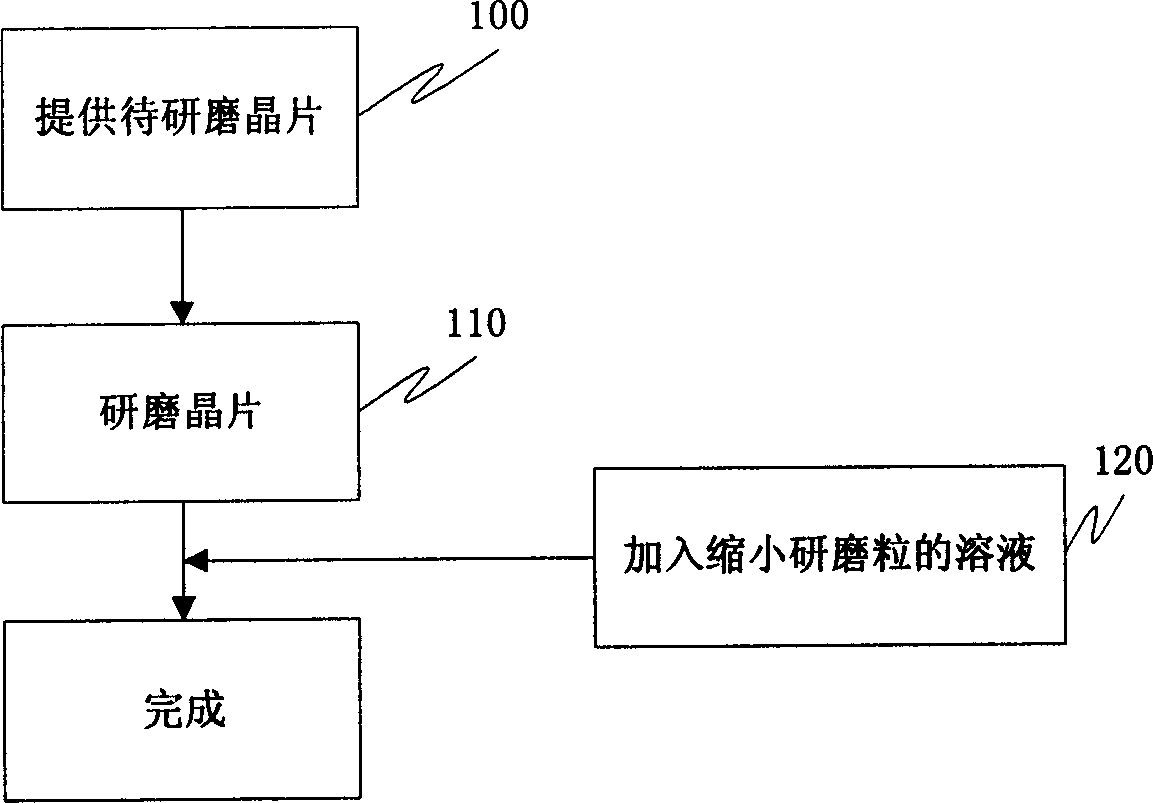
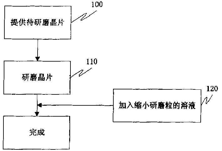
[0018] figure 1 It is a step diagram of a non-scratch chemical mechanical polishing (CMP) process according to a first embodiment of the present invention.

[0019] Please refer to figure 1 , in step 100, a wafer to be ground is provided. Then, in step 110, the wafer is ground, wherein the slurry used for grinding the wafer contains abrasive particles, such as silica particle abrasive particles.

[0020] Then, in step 120, a solution that can reduce the abrasive grain is added to reduce the size of the abrasive grain, thereby reducing the probability of the wafer surface being scratched, wherein the solution that can reduce the abrasive grain is, for example, potassium hydroxide (KOH) solution; for example For example, when the concentration of potassium hydroxide solution added is about 1M, the pH value of the abrasive will gradually change from 10 to about 12, and the particle size of the abrasive particles will also be reduced from 130 nanometers. Moreover, in order to o...

no. 2 example

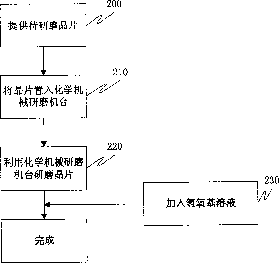
[0024] figure 2 It is a step diagram of a non-scratch chemical mechanical polishing process according to a second embodiment of the present invention, mainly using a chemical mechanical polishing machine for polishing.

[0025] Please refer to figure 2 , in step 200, a wafer to be ground is provided. Then, in step 210, the wafer is placed into a chemical mechanical polishing machine station to prepare for polishing. Subsequently, in step 220, the wafer is ground by using a chemical mechanical polishing machine, wherein the abrasive used for grinding the wafer contains silicon dioxide abrasive grains. Then, in step 230, a hydroxide solution is added, wherein the hydroxide solution is, for example, potassium hydroxide (KOH) solution; for example, when the concentration of the potassium hydroxide solution added is about 1M, the pH of the abrasive Will gradually change to greater than 10, while the size of the abrasive particles will also be reduced. Moreover, in order to ob...


PUM


Abstract

The invented technique uses abrasive containing the grind grain of silicon dioxide to grind a layer to be ground on substrate. A solution capable of reducing size of grind grain is added to the grinding procedure when the procedure is close to end in order to prevent surfaces of wafers from scoring.

Description

technical field [0001] The present invention relates to a semiconductor process, and more particularly to a nonscratch chemical mechanical polishing (CMP). Background technique [0002] At present, the chemical mechanical grinding process has been widely used in the planarizing or smoothing technology of the insulating layer surface. It mainly uses the mechanical grinding principle similar to "sharpening a knife" and cooperates with appropriate chemical additives. (reagent), a planarization technology that "smooths" the contours of the wafer surface with ups and downs. In the basic chemical mechanical polishing process, the wafer to be polished is placed in a chemical mechanical polishing machine, and chemical additives are added during grinding, the so-called abrasive (slurry), which contains abrasive grains with extremely high hardness. . [0003] However, although the above-mentioned chemical mechanical polishing process can keep the removal rate (removing rate) stable ...

Claims


Application Information

Patent Timeline
Patent Type & Authority Applications(China)
IPC IPC(8): H01L21/302
Inventor 刘裕腾
Owner MACRONIX INT CO LTD
Why Eureka
Try Eureka