
Method for forming grid electrode of semiconductor

A semiconductor and gate technology, applied in the field of semiconductor device formation, can solve problems that affect reliability, failure, and reduce gate coupling rate, so as to prevent reliability, increase gate coupling rate, and expand error margins. Effect

Inactive Publication Date: 2004-03-10
MACRONIX INT CO LTD
View PDF0 Cites 0 Cited by
  • Summary
  • Abstract
  • Description
  • Claims
  • Application Information

AI Technical Summary

Problems solved by technology

[0003] However, the above-mentioned method of forming a semiconductor gate is prone to defects in the interface between the high-density plasma oxide layer and the gate, and there is a risk of penetrating through the substrate when forming a larger upper portion of the gate subsequently, resulting in a single Bit (single bit) failure, thereby affecting its reliability (reliability)
Moreover, when semiconductor devices are miniaturized, in order to achieve the purpose of increasing the upper surface of the gate and reducing the size of the device at the same time, the distance between the two gates must be shortened as much as possible, so it is easy to cause misalignment in the subsequent lithography manufacturing process. Device failure caused by (mis-alignment), thereby reducing the gate coupling ratio (GCR for short)

Method used


Image

  • Method for forming grid electrode of semiconductor
  • Method for forming grid electrode of semiconductor
  • Method for forming grid electrode of semiconductor

Examples


no. 2 example

[0030] Figure 2A to Figure 2E It is a sectional view of the manufacturing process of the floating gate of the flash memory according to a second embodiment of the present invention.

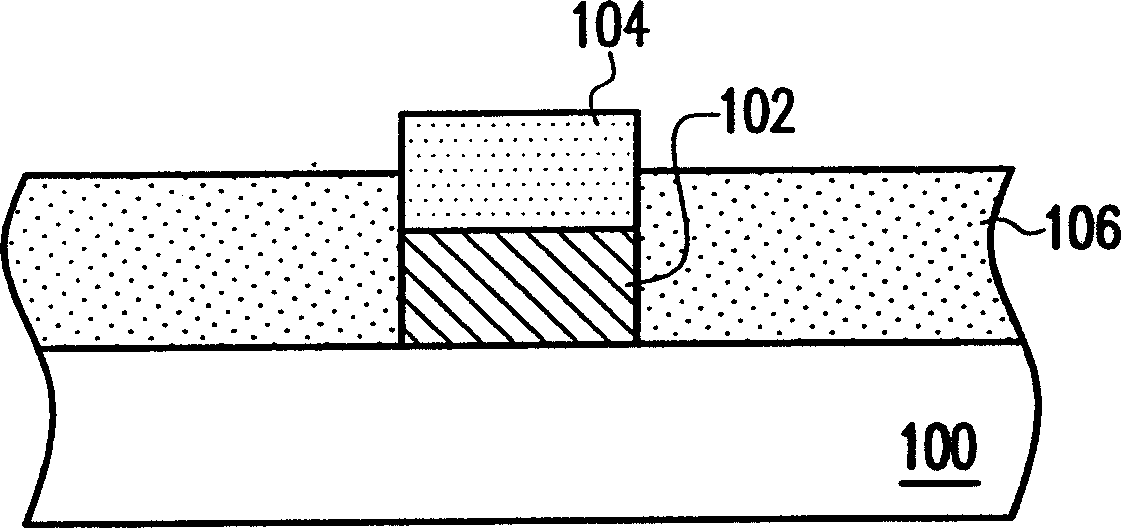
[0031] Please refer to Figure 2A , forming a stack structure comprising a conductor layer 202 and a top cover layer 204 on a substrate 200, wherein the conductor layer 202 is, for example, a polysilicon layer, and the top cover layer 204 is, for example, a silicon nitride layer, and the substrate 200 and the conductor A tunnel oxide layer (not shown) is also included between the layers 202 . Then, a high-density plasma dielectric layer 206 is formed on the substrate 200 and the top cover layer 204 is exposed, wherein the top of the high-density plasma dielectric layer 206 is higher than the top of the conductive layer 202, and its material is, for example, selected from silicon oxide ethnic groups.

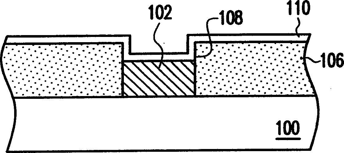
[0032] Then, please refer to Figure 2B , use such as hot phosphoric acid to cover the top ...


PUM


Abstract

First, a stack architecture including a conductor layer and a topping layer is formed on substrate. Next, a high-density plasma dielectric layer is formed and the topping layer is exposed, and top part of the high-density plasma dielectric layer is higher than the top part of the conductor layer. Then, the topping layer is removed. A concavity part is formed on the conductor layer since the high-density plasma dielectric layer is higher than the top part of the conductor layer. Finally, oxidation gap wall is formed sidewall at concavity part. A conductor layer deposited on substrate and covering the concavity part is connected to original conductor layer so as to form a grid electrode of a semiconductor device.

Description

technical field [0001] The present invention relates to a method for forming a semiconductor device, and in particular to a method for forming a semiconductor gate. Background technique [0002] At present, in the semiconductor manufacturing process, there is a gate manufacturing method that does not require chemical mechanical polishing (CMP) as a planarization process, and has gradually attracted attention due to its advantages of environmental protection and low cost. This method of manufacturing a semiconductor gate mainly utilizes a cap layer formed on the gate, cooperates with a high density plasma (HDP) oxide layer deposited on the substrate, and then uses hydrogen fluoride to (HF) Remove part of the high-density plasma oxide layer until the top cover layer is exposed, and then use the step of removing the top cover layer to remove the redundant high-density plasma oxide layer on the gate to obtain a flat surface with high density Plasma oxide layer. Moreover, after...

Claims


Application Information

Patent Timeline
IPC IPC(8): H01L21/28
Inventor 邱宏裕陈铭祥曾铕寪
Owner MACRONIX INT CO LTD
Features
  • Generate Ideas
  • Intellectual Property
  • Life Sciences
  • Materials
  • Tech Scout
  • Unparalleled Data Quality
  • Higher Quality Content
  • 60% Fewer Hallucinations
Learn More